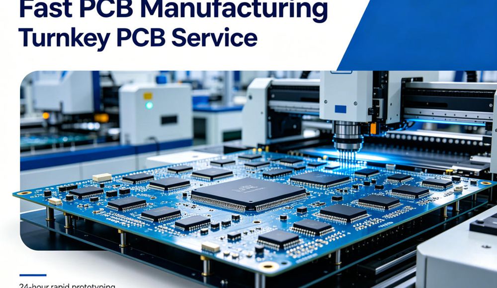
The rise of 5G standalone networks, AI servers, and high-performance computing (HPC) is redefining electronics manufacturing—and at the heart of this revolution is high-speed PCB technology. In 2026, high-speed PCB for 5G & AI isn’t just a component; it’s the critical foundation enabling ultra-fast data transmission, low latency, and massive computational power. As 5G-A rolls out globally and AI models demand 10x more bandwidth, high-speed PCB design and manufacturing are undergoing unprecedented innovation to meet these demands.
1. 5G & AI: The Driving Forces Behind High-Speed PCB Demand
By 2026, 60% of multilayer PCBs will serve 5G infrastructure and AI data centers (Prismark). 5G base stations, 1.6T/2.4T switches, and AI server motherboards (e.g., Nvidia Rubin architecture) require high-speed PCBs capable of 224Gbps+ signal transmission, low latency (<50ns), and minimal signal loss. AI accelerators, HBM (High-Bandwidth Memory) modules, and 5G millimeter-wave (mmWave) systems depend on precise impedance control, low-Dk materials, and advanced routing to maintain signal integrity at GHz frequencies. Without cutting-edge high-speed PCB solutions, 5G’s full potential and AI’s computational power would be unreachable.
2. Key Material Innovations for 2026 High-Speed PCBs
Material science is the backbone of high-speed PCB for 5G & AI in 2026. Traditional FR-4 substrates can’t support 5G/AI’s high-frequency demands—so manufacturers are adopting:
- Low-loss/high-frequency materials: Rogers RO4000, PTFE, and M9-grade laminates with Dk <3.5 and Df ≤0.002@10GHz, reducing signal attenuation by 45% vs. standard materials.
- Ultra-thin, low-roughness copper foils: HVLP4 and ultra-smooth copper (Ra <0.5μm) minimize signal reflection at 28GHz+, critical for 5G mmWave and AI SerDes channels.
- Thermally stable substrates: Materials with matched CTE (Coefficient of Thermal Expansion) prevent warping in AI servers, where temperatures reach 125°C+.
3. Advanced Design & Manufacturing Technologies
2026 high-speed PCB production relies on breakthrough technologies to handle 5G/AI’s complexity:
- Ultra-HDI & Any-Layer Interconnect: 3+ order blind/buried vias (≤50μm) and 0.1mm microvias enable 200+ lines/cm² routing density—essential for packing 8+ AI chips on a single board.
- Precision Impedance Control: ±3% tolerance (vs. industry standard ±5%) via TDR testing and AI-driven EDA tools, ensuring 50/85Ω differential pairs for PCIe 5.0/6.0 and 224Gbps PAM4 signals.
- AI-Assisted Design: Machine learning optimizes trace routing, reduces crosstalk, and predicts signal integrity issues—cutting design cycles by 30% and improving yields to 99.2%.
- 3D & Rigid-Flex Integration: 3D stacking and rigid-flex PCBs shrink size by 40% for 5G small cells and AI edge devices, while shortening signal paths to reduce latency.
4. Critical Challenges & Solutions in 2026
High-speed PCB for 5G & AI faces unique hurdles in 2026—and manufacturers are solving them:
- Signal Integrity (SI) & EMI: Advanced shielding, differential pair routing, and via-in-pad designs eliminate crosstalk and electromagnetic interference in dense 5G/AI layouts.
- Thermal Management: Thick copper layers (2oz+), thermal vias, and metal-core substrates dissipate heat from high-power AI chips, preventing performance throttling.
- Supply Chain for High-End Materials: Leading PCB & PCBA manufacturing partners secure long-term contracts for low-loss laminates and specialty copper, avoiding shortages plaguing the industry.
5. Applications: Where High-Speed PCBs Shine in 2026
- 5G Infrastructure: 16–32 layer high-speed PCBs for base stations and optical modules (400G/800G) enable SA 5G and low-latency V2X communication.
- AI Servers & Data Centers: 78-layer backplanes and GPU motherboards power next-gen AI training, supporting HBM and 10T+ data throughput.
- Automotive & ADAS: 77GHz radar high-speed PCBs enable L4 autonomous driving, with automotive-grade reliability (-40°C to +125°C).
- Edge AI & IoT: Miniaturized high-speed PCBs bring AI inference to smartphones, wearables, and industrial sensors with low power consumption.
The Future Beyond 2026: 6G & Next-Gen AI
Looking ahead, high-speed PCB innovation will accelerate for 6G (300GHz–3THz) and exascale AI. Graphene-enhanced substrates (Dk≈2.0), embedded passives, and terahertz testing will become standard, pushing signal speeds to 1Tbps+. Manufacturers investing in high-speed PCB for 5G & AI today will lead the 6G era tomorrow.
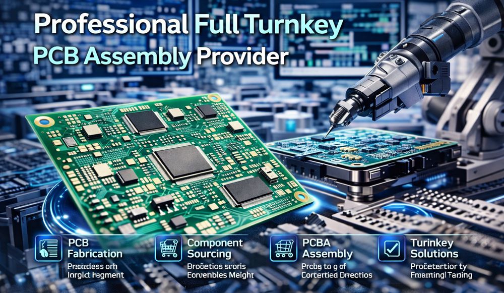
Partner with Ring PCB for High-Speed PCB Excellence
In 2026, high-speed PCB isn’t just about technology—it’s about partnering with experts who understand 5G and AI’s unique demands. At Ring PCB, we specialize in high-speed PCB design and manufacturing for 5G, AI, and advanced electronics, with IPC Class 3 certification, low-loss material expertise, and AI-driven quality control.