Ring PCB – Fast Prototype & Full Turnkey PCB PCBA One-Stop Solution
Product Description:
1.What are HDI PCB (High-Density Interconnect PCB)?
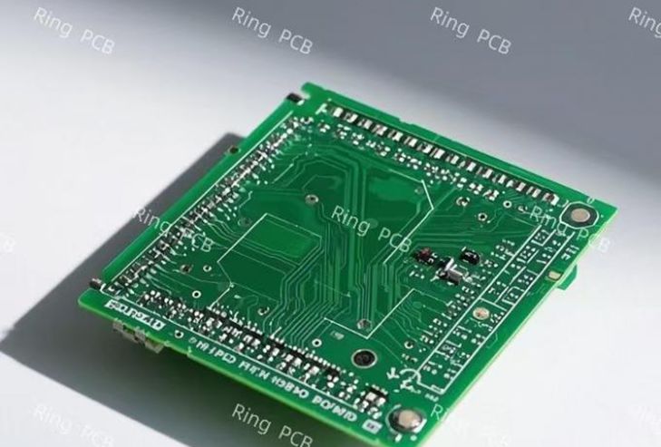
An HDI PCB (High-Density Interconnect PCB) is a type of PCB that features a higher wiring density per unit area compared to conventional PCBs. HDI PCBs use advanced technology, including micro-vias, blind and buried vias, and laser- drilled vias, to support complex designs with more interconnections. These design elements allow for more components to fit in smaller spaces, making HDI PCBs ideal for modern electronics where miniaturization, performance, and functionality are critical.
2.The product characteristics of HDI PCBs are as follows:
Compact design: The use of micro – vias, blind vias, and buried vias reduces the board space significantly. It can simplify an 8 – layer through – hole PCB to a 4 – layer HDI PCB with the same functions, helping to reduce the size and weight of electronic products.
Excellent signal integrity: The small vias reduce stray capacitance and inductance. The technology of incorporating blind vias and via – in – pad shortens the signal path, leading to faster signal transmission and better signal quality.
High reliability: HDI technology makes routing and connection easier, and offers PCBs better durability and reliability in harsh conditions and extreme environments.
Cost effective: When the number of PCB layers exceeds 8, using HDI technology can reduce manufacturing costs while maintaining functionality.
High wiring density: HDI PCBs have finer lines, smaller holes, and a higher density than conventional PCBs. They can realize more complex circuit designs and are suitable for chips with many pins in mobile devices and other high – tech products.
3.Challenges of HDI PCB Manufacturing
Challenge 1: Precision Drilling for Micro-Vias
Micro-vias, which are often less than 150 microns in diameter, are a fundamental element in HDI PCBs. They enable denser routing of interconnections, but drilling these tiny holes with high precision is a major challenge. Inadequate precision in drilling can lead to misalignments, electrical instability, and increased costs due to production errors.
Solution
Ring PCB uses advanced laser drilling technology to create micro-vias with the precision required for reliable HDI designs. Our high-precision laser drills are calibrated to deliver consistent, accurate results, even on multi-layer boards. This capability minimizes misalignments and defects, resulting in stronger electrical connections and more reliable boards.
Challenge 2: Managing Layer Stacking and Alignment
HDI PCBs often require multiple layers to accommodate complex routing and additional components within limited space. Additionally, layer stacking for HDI boards involves using different types of vias, including blind and buried vias.
Solution
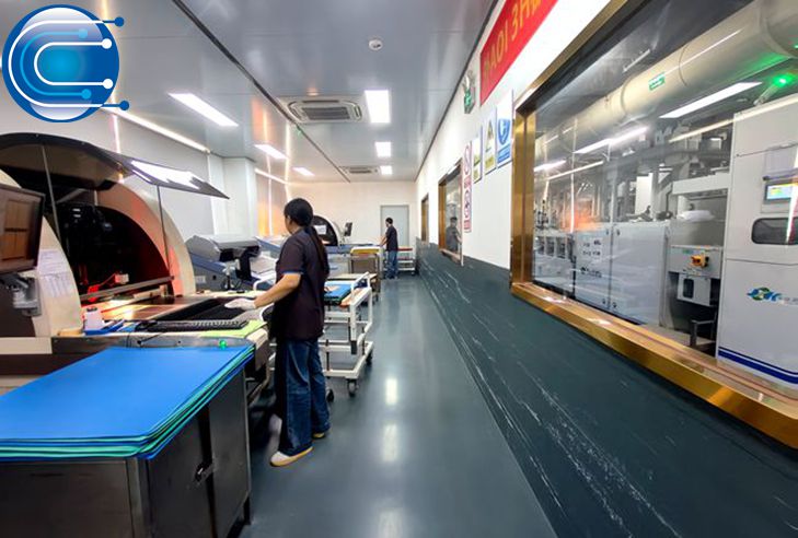
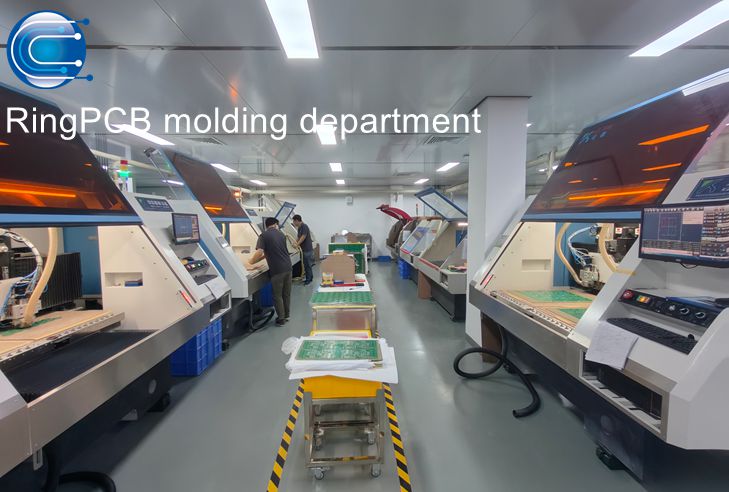
Our Shenzhen facility is equipped with advanced layer stacking technology that enables precise alignment and lamination. Using automated alignment systems and high-precision lamination, we ensure each layer aligns perfectly. We also use optical alignment verification to confirm that all layers are positioned correctly, preventing costly misalignment.
Challenge 3: Minimizing Signal Integrity Issues
As electronic devices become more compact and complex, HDI PCBs must support high-speed, high-frequency signals without compromising signal integrity. Factors like crosstalk, electromagnetic interference (EMI), and signal loss can all affect the performance of HDI PCBs, especially in applications that demand high-speed data processing.
Solution
At Ring PCB, we incorporate impedance control and isolation techniques into our HDI designs to mitigate signal integrity issues. By carefully controlling the spacing of traces and managing the impedance levels, we reduce crosstalk and EMI. Our design team collaborates with customers to optimize layout and layer configuration to ensure that high-speed signals travel seamlessly, maintaining signal strength and clarity throughout the PCB.
Challenge 4: Reliable Copper Plating for Micro-Vias
For HDI PCBs, plating micro-vias with copper is a delicate process. The plating must be uniform and defect-free, as any inconsistencies in copper thickness can lead to performance issues or early board failure. In HDI manufacturing, achieving uniform plating in such small features requires specialized equipment and precise process control.
Solution
Our equipment provides uniform copper deposition even in tiny vias, ensuring each connection is strong and conductive. Additionally, we monitor plating thickness using advanced inspection systems, verifying that every micro-via meets the exacting standards.
Challenge 5: Ensuring Thermal Management
As HDI PCBs support more functionality in smaller spaces, managing heat becomes a critical concern. The density of components and the close spacing of layers increase the risk of heat buildup, which can lead to performance degradation or failure.
Solution
To address thermal management challenges, we use materials with high thermal conductivity to optimize heat dissipation. We employ thermal vias and heat sinks to manage heat flow across the PCB.
Challenge 6: Quality Control in HDI Production
Manufacturing HDI PCBs requires a highly controlled environment and strict quality assurance. The complexity and density of HDI boards mean that even minor defects can result in significant functional issues.
Solution
We use Automatic Optical Inspection (AOI), X-ray inspection, and Electrical Testing (ET) to identify potential issues in real-time. Our quality assurance team monitors each stage of production to ensure that our HDI PCBs are free of defects and meet our high standards for performance and reliability.
One-Stop Service for PCB and PCBA Solutions!
Ring PCB’s Key Advantages
-
Advanced Engineering for Precision PCB Manufacturing
-
High-Density Stack-Up: 2-48 layer boards, ideal for 5G, industrial control, medical devices, and automotive electronics.
-
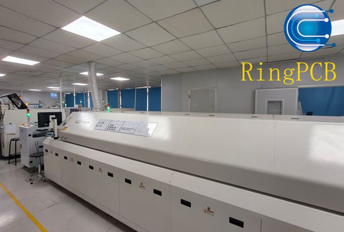
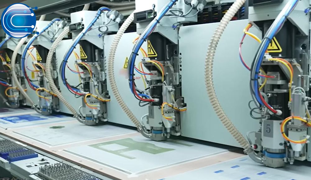
Smart Manufacturing: Self-owned facilities with LDI laser exposure, vacuum lamination, and flying probe testers, ensuring compliance with IPC-6012 Class 3 standards.
-
-
Integrated PCBA Services | One-Stop Turnkey Solutions
-
Full Assembly Support: PCB fabrication, component sourcing, SMT assembly, and functional testing, all under one roof.
-
DFM/DFA Optimization: Our expert engineering team optimizes designs to reduce risks and BOM costs, enhancing efficiency.
-
Rigorous Quality Control: X-ray inspection, AOI testing, and 100% functional validation ensure zero-defect delivery.
-
-
Self-Owned Factory with Full Supply Chain Control
-
Vertical Integration: We manage raw material procurement, production, and testing in-house, ensuring maximum control over the production process.
-
Triple Quality Assurance: AOI, impedance testing, and thermal cycling with a defect rate of <0.2% (industry average: <1%).
-
Global Certifications: ISO9001, IATF16949, and RoHS compliance to meet international standards.
-
Why Choose Ring PCB?
-
18Years of Excellence in PCB and PCBA manufacturing, offering high-quality, reliable products for critical applications.
-
Self-Owned Factories ensure full control over the production process, allowing us to meet strict deadlines and guarantee consistent quality.
-
End-to-End Technical Support: From design and prototyping to mass production and final assembly, we provide comprehensive support at every stage.
-
Fast Turnaround: Prototype production within 3 days and mass production within 7 days to keep your projects on schedule.
-
Global Reach: Serving customers in over 50 countries with ongoing industrial partnerships.
Contact Us
📧 Email: rfq@ringpcb.com


")