The global shift toward higher power density hardware — including high-speed EV chargers, grid-tied inverters and industrial motor drives — raises stricter requirements for high power PCBA performance. Industry statistics indicate that over 55% of field failures on power electronics equipment originate from thermal imbalance and assembly defects on PCBA. Unlike standard circuit assemblies, high power PCBA carries continuous large currents, generating substantial heat; repeated thermal cycling creates thermal stress that leads to solder joint cracks, substrate delamination and trace degradation. Professional Electronic Manufacturing Services (EMS) implement targeted process controls to overcome these reliability obstacles. This article breaks down key technical challenges and the EMS solutions that protect your product’s long-term operational stability.
1. Primary Reliability Threats for High Power PCBA
1.1 Excessive Heat Accumulation and Thermal Cycling Stress
High-current flow creates I²R heat loss on copper traces. Without effective thermal design and precise assembly, local hotspots form around power chips. Each 10°C temperature rise reduces the service life of semiconductor components by approximately half. When equipment cycles between standby and full-load operation, alternating expansion and contraction generates mechanical stress on solder joints of IGBT, MOSFET and high-current connectors.
Many design teams complete PCB layout with thermal simulation but overlook manufacturing factors. Poor solder paste printing, uneven reflow temperature curves or improper torque during power component installation will turn theoretical thermal designs into unreliable finished boards.
1.2 High Voltage Creepage, Clearance and EMC Risks
High power PCBA often works under hundreds of volts DC or AC. Insufficient creepage distance, flux residue after assembly and uncontrolled trace spacing can trigger partial discharge or short-circuit faults. Meanwhile, fast switching of SiC/GaN power devices produces strong electromagnetic interference, which requires optimized grounding layout and controlled assembly processes to avoid EMC certification failures.
1.3 Compatibility with Heavy Copper PCB Structures
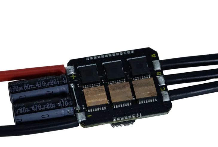
Most high power systems adopt heavy copper PCB from 3oz to 12oz. Thick copper layers bring assembly challenges: uneven heat transfer during reflow soldering, increased risk of thermal voids under large power components, and difficulty controlling flatness of the baseboard. General EMS workshops without heavy copper assembly experience struggle to maintain stable yields.
2. Professional EMS Strategies to Improve High Power PCBA Reliability
2.1 Customized Assembly Process for Thermal Control
Qualified EMS providers adjust reflow profiles specifically for heavy copper boards. Thick copper absorbs more heat, requiring optimized temperature ramp rates to prevent cold solder or overheating of sensitive semiconductors. For high-power surface-mount devices, precise solder paste volume control reduces void ratios, which directly improves heat conduction.
At Ring PCB, our production team develops dedicated soldering profiles for heavy copper high power PCBA. All assemblies pass X-Ray inspection to check void levels under power chips, together with AOI and in-circuit testing to eliminate hidden assembly defects.
2.2 Strict Cleaning and Residue Management
Flux residue left on high-voltage circuits easily causes electrochemical migration under humid operating conditions. We implement standardized ultrasonic cleaning or inline plasma cleaning processes for high power PCBA that will be used in outdoor or high-humidity environments. This critical step is often skipped by low-cost assembly suppliers.
2.3 Comprehensive Validation Testing Protocols
Beyond basic electrical tests, high power PCBA requires application-oriented verification. Leading EMS providers offer optional thermal cycling testing, humidity testing and simulated full-load aging tests to expose latent defects before shipment. These screening procedures effectively reduce warranty costs after product launch.
3. Why Early EMS Involvement Improves Long-Term Reliability
Many OEMs only engage assembly manufacturers after design finalization. However, EMS engineers can propose practical improvements during the design phase: adjusting component placement to optimize heat dissipation, modifying pad geometry for power devices, and recommending suitable copper thickness to balance performance and manufacturing cost. Early collaboration avoids costly redesign after prototypes are completed.
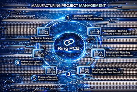
Ring PCB encourages customers to share preliminary design files for free DFM review. Our combined PCB and assembly engineering team identifies manufacturability and thermal risks in advance, optimizing the design for high-volume, reliable production.
Conclusion
Thermal stress, assembly voids, EMC risks and heavy copper process barriers create unique reliability challenges for high power PCBA. Simply finishing component soldering is not sufficient; manufacturers must adopt customized processes, strict cleaning and multi-stage reliability testing. Partnering with an experienced EMS provider specialized in power electronics minimizes field failure risks and protects your brand reputation.
If you are developing high power PCBA that demands superior thermal performance and long-term reliability, share your project documents with our engineering team at rfq@ringpcb.com to receive professional manufacturing recommendations and pricing.