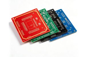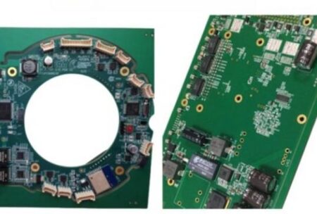
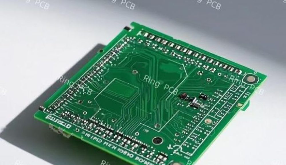
HDI PCB technology helps you fit more circuitry into smaller electronic devices without sacrificing routing flexibility or signal performance. However, manufacturing high-density boards requires precise microvia drilling, reliable copper plating, accurate layer alignment, and effective quality control. Without these controls, you may face connectivity defects, signal integrity problems, or delays during assembly.
If you are developing compact industrial controllers, medical electronics, automotive systems, or high-speed communication equipment, choosing the right manufacturing partner matters. Ring PCB, founded in Shenzhen, China, in 2008, provides PCB fabrication and full-turnkey PCBA services. With a 10,000 m² self-owned facility, a team of 500 employees, and production capacity of 50,000 m² of bare PCBs per month, Ring PCB supports projects from rapid prototyping to volume production.
What Is an HDI PCB?
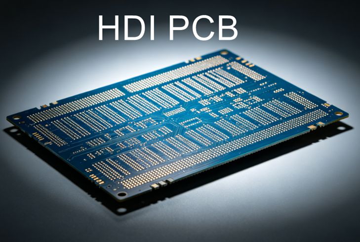
An HDI PCB (High-Density Interconnect Printed Circuit Board) uses finer circuit lines, smaller vias, and higher connection density than conventional PCB designs. It commonly incorporates laser-drilled microvias, blind vias, buried vias, and via-in-pad structures to connect components across different layers.
These features allow you to optimize board size, component placement, and electrical routing. Depending on your design requirements, HDI technology can also reduce the number of layers needed compared with a conventional through-hole design.
Typical applications include:
- Consumer electronics: Compact devices with limited internal space.
- Medical equipment: Dense control circuits requiring reliable interconnections.
- Industrial automation: Controllers, sensors, and embedded systems.
- Automotive electronics: Electronic modules with demanding packaging requirements.
- Communication equipment: Designs requiring controlled impedance and high-speed signal routing.
Key Benefits of HDI PCB Technology
1. Higher Wiring Density
Microvias and finer traces enable more connections within a limited board area. Consequently, you can accommodate complex circuitry without increasing the overall dimensions of your electronic product.
2. Improved Signal Integrity
Shorter interconnections can help reduce parasitic capacitance and inductance. When your application requires high-speed signals, controlled impedance, suitable trace spacing, and an appropriate stack-up are essential to managing signal loss and crosstalk.
3. More Flexible Board Design
Blind and buried vias provide additional routing options while preserving usable surface area. This flexibility is particularly useful when your design combines fine-pitch components with multiple functional layers.
4. Potential Cost and Space Savings
HDI technology may reduce board size or simplify a design that would otherwise require more conventional PCB layers. However, microvia processing and sequential lamination add manufacturing complexity, so the final cost depends on your stack-up, material selection, production volume, and yield requirements.
HDI PCB vs. Conventional Multilayer PCB
The right choice depends on your circuit density, component pitch, performance targets, and budget.
| Comparison | HDI PCB | Conventional Multilayer PCB |
|---|---|---|
| Via technology | Microvias, blind and buried vias as required | Primarily through-hole vias |
| Routing density | High | Depends on line width, spacing, and layer count |
| Board size | Can support more compact layouts | May require more space for complex routing |
| Manufacturing | Requires precise microvia and lamination processes | Generally uses more conventional fabrication processes |
| Cost considerations | Higher process complexity; savings depend on design | May be economical for less dense circuits |
| Typical applications | Compact, high-density electronics | Industrial control boards and general electronics |
How Ring PCB Manufactures HDI Circuit Boards
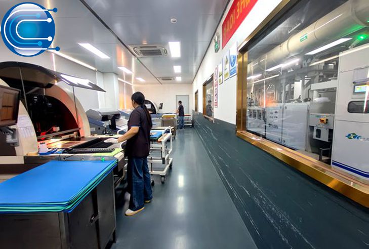
Reliable HDI PCB fabrication depends on controlling each production stage. Ring PCB combines in-house manufacturing capabilities with inspection processes to support demanding multilayer designs.
Key manufacturing capabilities include:
- Laser drilling: Creates microvias for high-density interconnections.
- Layer alignment and lamination: Maintains registration across multilayer structures.
- Copper plating: Establishes conductive connections within drilled vias.
- LDI exposure: Supports precise circuit pattern formation.
- AOI and X-ray inspection: Helps identify circuit pattern defects and hidden connection issues.
- Electrical testing: Checks board connectivity against the specified electrical requirements.
Ring PCB operates under ISO 9001, ISO 14001, ISO 13485, and IATF 16949 management system certifications and holds UL certification. These credentials support quality management across relevant manufacturing applications; specific product and project requirements should be confirmed before ordering.
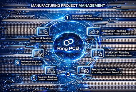
How to Order a Custom HDI PCB
Follow these steps to move from design requirements to production.
- Prepare your design files. Provide Gerber or other accepted manufacturing files, drill data, stack-up information, and fabrication notes.
- Confirm technical specifications. Define the layer count, board dimensions, copper thickness, materials, microvia geometry, impedance requirements, and surface finish.
- Complete DFM review. Ask your manufacturer to check manufacturability, via structures, clearances, and potential design risks before production.
- Approve the quotation and prototype. Confirm pricing, sample quantities, lead time, inspection criteria, and any required engineering changes.
- Proceed to assembly and testing. If you need finished boards, coordinate component sourcing, SMT or through-hole assembly, and functional testing.
Ring PCB offers a minimum order quantity of one unit for supported projects. Its general capabilities include prototype production within three days, while the featured 2–12 layer HDI PCB product lists a delivery time of 7–14 working days. Confirm the actual schedule against your design complexity, order quantity, component availability, and required testing.
FAQ
What layer counts can Ring PCB manufacture?
The featured HDI PCB product supports 2–12 layers. Ring PCB also reports multilayer PCB manufacturing capability of up to 62 layers across its broader product range. Confirm the available stack-up and HDI structures for your specific design.
Can Ring PCB provide HDI PCB assembly services?
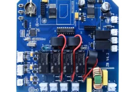
Yes. Ring PCB provides PCB fabrication, component sourcing, SMT and through-hole assembly, testing, and turnkey PCBA services. This integrated approach can simplify supplier coordination and production planning.
What information is needed for an HDI PCB quotation?
Provide your design files, layer count, board dimensions, quantity, material requirements, surface finish, microvia specifications, impedance requirements, and assembly needs. These details help the engineering team evaluate manufacturability and prepare a more accurate quotation.
Conclusion
Choosing the right HDI PCB manufacturer helps you balance circuit density, electrical performance, manufacturability, and project cost. Ring PCB combines 18 years of PCB and PCBA manufacturing experience with a self-owned Shenzhen facility, multilayer fabrication capabilities, and integrated assembly services to support projects from prototype development to mass production.
Request a Custom HDI PCB Quote
Send your Gerber files, layer stack-up, quantity, and assembly requirements to Ring PCB. Contact the engineering team at rfq@ringpcb.com to discuss design-for-manufacturing review, lead time, and a quotation tailored to your project.