| Place Of Origin: | Shenzhen, China | Certification: | ISO9001, ISO14001, ISO13485, and IATF16949. |
| Type: | Communication PCBA | Board Thickness: | Usually 0.8 - 2.4mm |
| Line Width/Spacing: | Commonly 0.1 - 0.3mm / 0.1 - 0.3mm | Surface Finish: | ENIG (Electroless Nickel Immersion Gold), HASL (Hot - Air Solder Leveling), Etc. |
| Operating Temperature: | -40°C - 85°C | Signal Frequency: | Ranges From Low - Frequency (kHz) To High - Frequency (GHz) Depending On Application |
| Power Consumption: | Varies Widely Based On Components, E.g., A Few MW To Several W | Certifications: | IPC, RoHS, UL, ISO9001, ISO14001,ISO13485,IATF16949 |
| Testing And Inspection: | Automated Optical Inspection (AOI), X-ray Inspection | Assembly Accuracy: | Tolerance Within ±0.05 - 0.1mm For Component Placement |
| Insulation Resistance: | ≥1000MΩ | Other Service: | We Can Help With The Procurement Of Electronic Components On Behalf Of Customers. |
| Application Areas: | Are Used In A Wide Array Of Devices, Including: Base Stations For Mobile Networks. Routers And Modems For Internet Connectivity. Satellite Communication Systems For Global Coverage. Optical Networking Equipment For High-speed Data Transfer. | Packaging Details: | Vacuum packing+Cardboard packing case |
| Supply Ability: | 50000㎡per week | ||
| Highlight: | PCBA for communication device, communication device PCB manufacturer, fast prototype PCBA production | ||
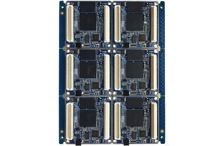
Product Overview
One-Stop PCB & PCBA Solutions for Communication Equipment
Ring PCB is a professional PCBA manufacturer for communication devices, providing end-to-end PCB fabrication and PCB assembly services — from fast prototyping to mass production.
With 17 years of manufacturing experience and a self-owned factory in Shenzhen, we support global customers with high-reliability, high-frequency communication PCBAs.
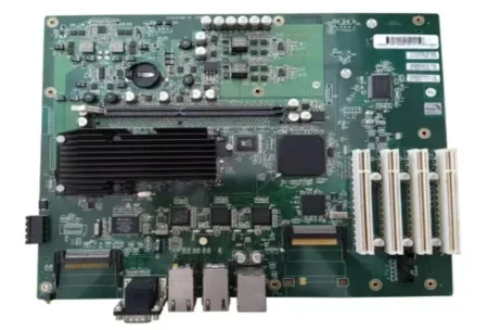
Our services cover routers, base stations, wireless modules, IoT devices, optical communication equipment, and other data transmission systems requiring stable signal integrity and long-term reliability.
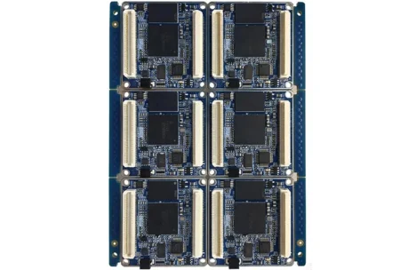
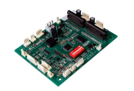
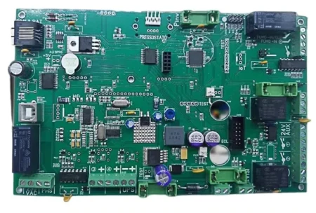
What Is Communication PCBA?
Communication PCBA (Printed Circuit Board Assembly) is a fully assembled PCB designed for signal transmission, processing, and reception in communication systems.
It integrates:
-
High-speed processors
-
RF and communication chips
-
Power management circuits
-
Connectors and interfaces
These assemblies form the core hardware platform of modern wired and wireless communication devices.
Key Characteristics of Communication PCBAs
High-Frequency Performance
Designed for GHz-level signal transmission with low loss and low interference.
High-Density & Miniaturization
HDI technology supports compact layouts, fine-pitch components, and multilayer designs.
Long-Term Reliability
Built to operate 24/7 under thermal stress, vibration, and complex environments.
Functional Integration
Combines data processing, modulation, demodulation, and protocol execution on a single board.
Flexible Customization
PCB stack-up, materials, impedance, and power design tailored to your application.
Communication PCBA Applications
Our PCBAs are widely used in:
-
Mobile network base stations
-
Routers & modems
-
Optical communication equipment
-
Satellite communication systems
-
IoT & smart devices
Manufacturing Challenges & Ring PCB Solutions
1. High-Speed Signal Integrity
Solution:
-
Controlled impedance PCB design
-
Low-loss materials (Rogers, Isola, Nelco)
-
TDR and impedance testing
2. Thermal Management
Solution:
-
Thermal vias & copper planes
-
Aluminum-based PCBs
-
8-stage lead-free reflow soldering
3. HDI & Multilayer Complexity
Solution:
-
Blind/buried vias & microvias
-
Up to 48-layer PCB manufacturing
-
Fine-line & fine-pitch SMT assembly
4. Environmental Resistance
Solution:
-
Conformal coating & encapsulation
-
Thermal shock & environmental testing
5. Power Efficiency
Solution:
-
Optimized copper thickness & routing
-
Efficient power management layouts
6. Regulatory Compliance
Solution:
-
RoHS & REACH compliant production
-
ISO9001 & IATF16949 certified factory
Common Technical Parameters
| Parameter | Specification |
|---|---|
| Board Thickness | 0.8 – 2.4 mm |
| Min Line Width / Spacing | 0.1 / 0.1 mm |
| PCB Layers | 2 – 48 Layers |
| Surface Finish | ENIG, HASL, OSP |
| Operating Temperature | -40°C to +85°C |
| Signal Frequency | kHz – GHz |
| Assembly Accuracy | ±0.05 – 0.1 mm |
| Insulation Resistance | ≥1000 MΩ |
| Assembly Type | SMT / THT / Mixed |
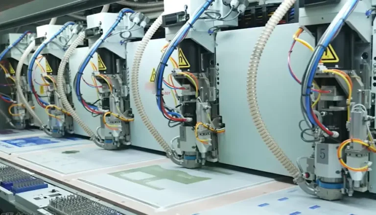
Why Choose Ring PCB?
17 Years of Industry Experience
Trusted by over 20,000 global customers.
One-Stop Turnkey PCBA Service
PCB fabrication + component sourcing + SMT/DIP assembly + testing.
Advanced Manufacturing Capability
LDI exposure, vacuum lamination, AOI, X-ray inspection, flying probe testing.
Self-Owned Factory & Full Process Control
Stable quality, fast delivery, competitive pricing.
Global Certifications
ISO9001, IATF16949, RoHS compliant.
Important Notice
-
All products are customized services. Please contact us before ordering.
-
Product images are real; minor color differences may occur due to lighting and display settings.
Contact Us
📧 Email: rfq@ringpcb.com