Product Description
What Is a Multilayer PCB?
A multilayer PCB (Printed Circuit Board) is composed of three or more conductive copper layers laminated together with insulating materials. Compared with single-sided or double-sided boards, multilayer PCB manufacturing enables higher circuit density, improved signal integrity, and more compact electronic designs.
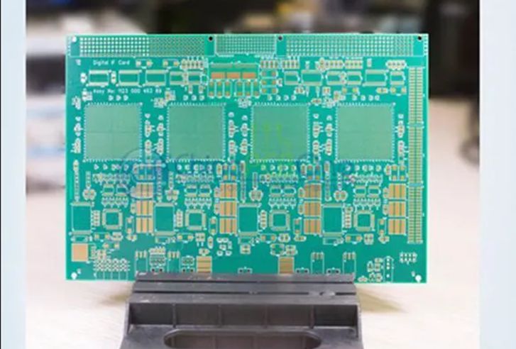
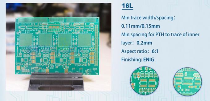
The multilayer PCB shown in the image is a customized solution manufactured for a customer project, presented for reference to demonstrate Ring PCB’s multilayer PCB manufacturing capabilities.
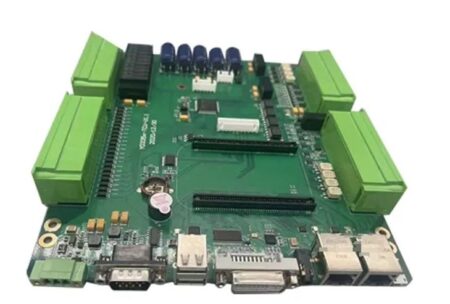
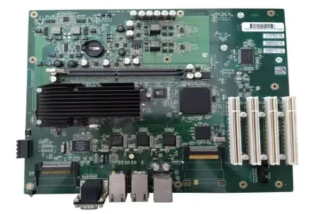
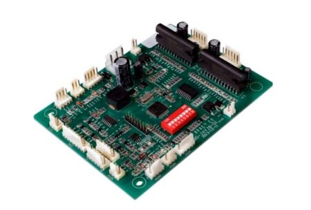
Multilayer PCBs are widely used in industrial control systems, communication equipment, power electronics, medical devices, automotive electronics, and high-performance embedded applications.
Key Features & Advantages of Multilayer PCB Manufacturing
High Circuit Density & Compact Design
Multilayer PCB manufacturing allows complex routing within limited space, supporting compact and highly integrated electronic products.
Stable Signal Integrity
Through precise stack-up design and impedance control, multilayer PCBs ensure stable signal transmission for high-speed and high-frequency applications.
Enhanced Power & Thermal Performance
Multiple copper layers improve power distribution and heat dissipation, enhancing overall system reliability and durability.
Flexible Customization
Ring PCB supports customized printed circuit board manufacturing, including different layer counts, materials, thicknesses, surface finishes, and special process requirements.
Manufacturing Challenges & Our Solutions
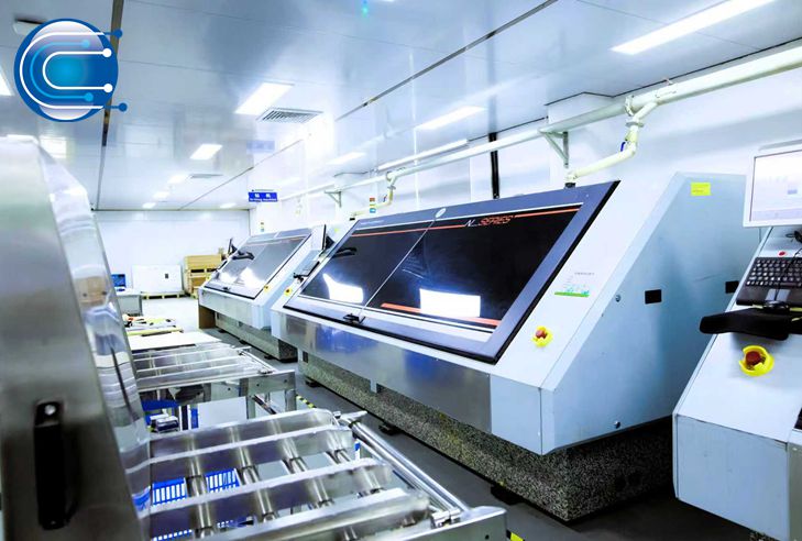
Producing high-quality multilayer PCBs involves technical challenges such as layer alignment accuracy, lamination stability, drilling precision, and impedance control.
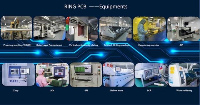
With 18 years of manufacturing experience, Ring PCB addresses these challenges through:
-
Advanced lamination and CNC drilling equipment
-
Controlled impedance production processes
-
Strict in-house quality inspection
-
Engineering support for DFM optimization
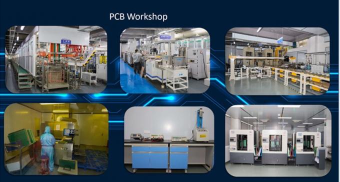
Our self-operated manufacturing facilities ensure stable quality, controlled lead times, and consistent performance from prototype to mass production.
Typical Technical Specifications (Reference)
| Item | Specification |
|---|---|
| Layer Count | 12 Layers |
| Base Material | FR4 TG170 |
| Board Thickness | 1.6 ± 0.16 mm |
| Min Trace Width / Spacing | 0.1 mm / 0.1 mm |
| Min PTH to Inner Layer Trace Spacing | 0.2 mm |
| Aspect Ratio | 8:1 |
| Surface Finishing | ENIG |
| Special Technology | Impedance Control |
| Single-ended Impedance | 50 ± 5 Ω |
| Differential Impedance | 100 ± 10 Ω |
Note:
The above parameters are for reference only. Actual specifications can be customized based on project requirements. Please contact Ring PCB’s professional team for technical consultation.
Why Choose Ring PCB?
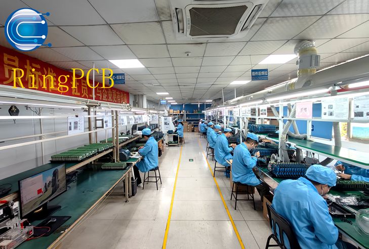
Ring PCB is a professional PCB and PCB assembly manufacturer with 18 years of industry experience. We operate modern, self-owned manufacturing facilities in Shenzhen and Zhuhai, covering approximately 10,000 square meters, supported by a skilled team of 500 employees.
All PCB and PCBA products comply with international standards, including ISO9001, ISO14001, ISO13485, and IATF16949.
We support 3-day rapid prototyping and 7-day mass production, with products exported to over 50 countries and regions worldwide.
Whether you need multilayer PCB manufacturing or a complete full-turnkey PCBA solution, Ring PCB is your reliable manufacturing partner.
RingPCB16-Layer PCB Manufacturing
Contact Us
If you are looking for a reliable partner for multilayer PCB manufacturing, PCB assembly, or full turnkey PCBA services, Ring PCB offers fast prototyping and full turnkey one-stop solutions.
Contact Us for more inquriy
Email: rfq@ringpcb.com
website:https://www.ringpcb.com/