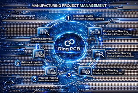
Full Turnkey PCBA Pre-Shipment Quality Control Process
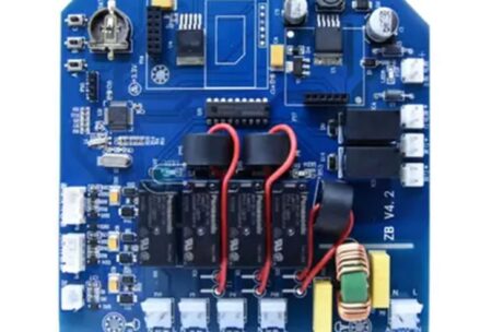
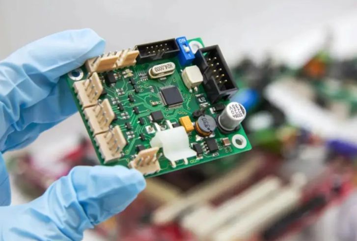
We provide a one-stop full turnkey PCB assembly service. In addition, we apply a strict multi-dimensional quality control system for all PCBA products. As a result, no board is shipped without completing all inspection procedures.
Moreover, we use Automated Optical Inspection (AOI) and X-ray testing as our core detection methods. Meanwhile, we combine functional testing and manual review to eliminate hidden defects.
Therefore, we ensure stable product quality for every shipment.
1. Introduction to Core Testing Equipment
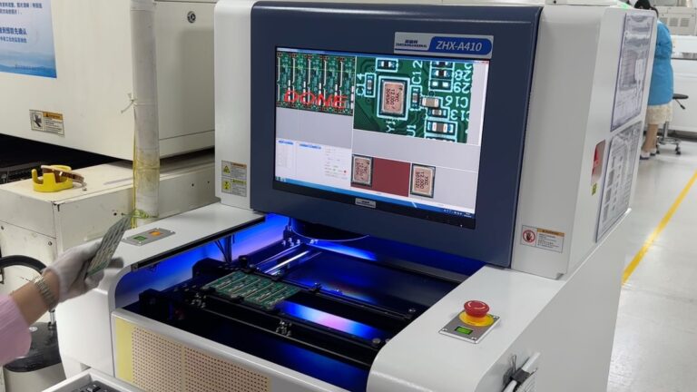
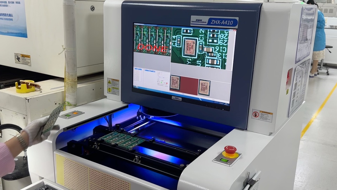
Automated Optical Inspection (AOI)
AOI is an intelligent inspection system used after SMT assembly. First, it captures high-resolution images of the PCB surface. Then, it compares the images with original design files using AI algorithms.
In addition, AOI quickly detects surface defects such as:
- missing components
- component misalignment
- tombstoning
- solder bridging
- insufficient solder
- excess solder
- surface scratches
As a result, defective boards are marked immediately and sent to rework. Therefore, we fix surface issues at an early production stage.
X-Ray Inspection
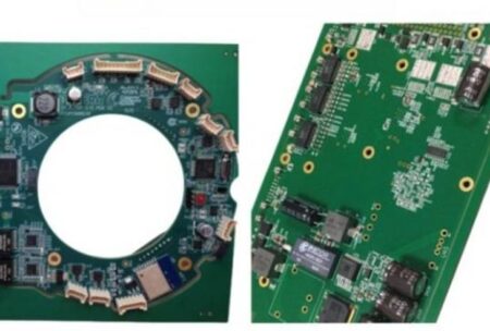
Unlike AOI, X-ray inspection checks internal solder joints. It focuses on hidden components such as BGA, QFN, and bottom-mounted chips.
First, X-ray equipment penetrates the PCB structure. Then, it generates internal solder images.
In addition, it detects hidden defects such as:
- BGA solder voids
- cold solder joints
- internal short circuits
- incomplete bonding
As a result, we ensure strong internal connection stability. Therefore, we prevent long-term failure caused by hidden solder defects.
2. Complete QC Procedures Before Shipment
Every PCBA must pass a strict sequence of quality checks.
Post-SMT AOI Inspection
First, we perform full surface inspection of all SMT components and solder joints.
X-Ray Inspection
Next, we scan all hidden solder joints in BGA and QFN components.
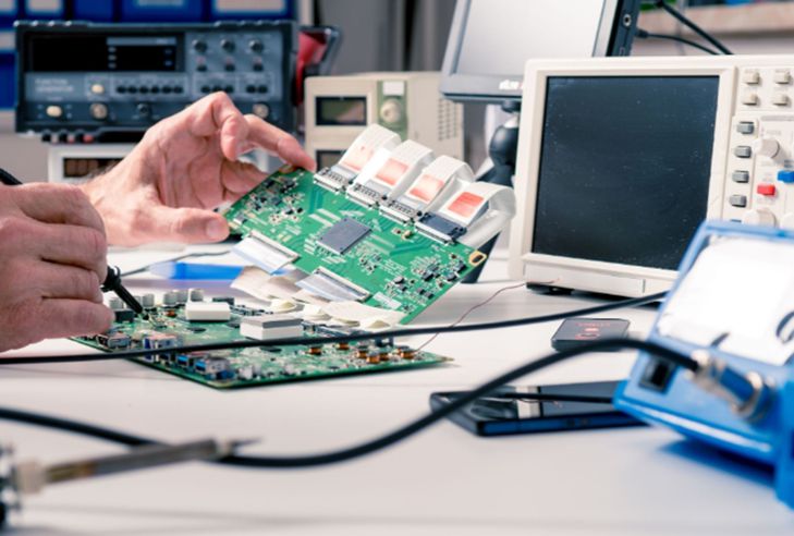
Manual Visual Recheck
In addition, trained inspectors perform secondary manual inspection. This helps catch minor defects missed by machines.
Functional Circuit Test (FCT)
Then, we simulate real working conditions of the product.
We test:
- power supply performance
- signal transmission
- circuit conduction
- customized functional requirements
As a result, only fully qualified boards move to the next stage.
Burn-in Aging Test (Optional)
Moreover, we run long-time power-on testing.
This process helps identify unstable components early. Therefore, we reduce long-term failure risk.
Final Appearance Inspection
In addition, we check:
- silkscreen quality
- labeling accuracy
- board cleanliness
- physical damage
Packing Audit
Finally, we verify:
- anti-static packaging
- order quantity
- shipping labels
- sealing condition
As a result, we ensure safe delivery.
3. Manufacturing Capability & Traceability
RingPCB has 18 years of full turnkey PCBA manufacturing experience. In addition, we handle PCB fabrication, component sourcing, SMT assembly, and testing in-house.
Therefore, we achieve full process control and batch traceability.
Moreover, we store all inspection data for quality tracking.
As a result, we meet strict requirements for:
- industrial control
- medical devices
- automotive electronics
- IoT systems
Email: rfq@ringpcb.com
Official Website: https://www.ringpcb.com