The global power electronics PCB market is projected to reach $18.7 billion in 2026, with heavy copper PCBs (≥3oz) accounting for 38% of total demand, driven by the rapid expansion of electric vehicle charging infrastructure, commercial energy storage systems, industrial inverters and AI server power supplies. As wide-bandgap (WBG) semiconductors like SiC and GaN enter mass adoption, high power supply systems are moving toward higher power density, faster switching speeds and stricter efficiency standards — creating unprecedented technical challenges for PCB design, fabrication and assembly.
For OEM procurement and engineering teams, 2026 brings a dual pressure: delivering higher performance power products while controlling long-term reliability risks and total cost of ownership. Generic circuit board vendors can no longer meet the complex requirements of modern high-power systems. Partnering with a provider that delivers integrated PCB and PCB assembly services with deep power electronics expertise has become a core competitive advantage for power supply brands.
This article analyzes the 2026 market landscape of high power supply applications, breaks down the top pain points facing B2B buyers, and explains how end-to-end PCB and PCB assembly services from a professional source factory like RingPCB address thermal stability, EMI compliance, manufacturing yield and supply chain resilience.
1. 2026 Market Drivers Reshaping High Power PCB Requirements
Four high-growth application sectors are pushing power supply PCB technology to new limits, and all share a common need for robust, thermally optimized PCB and PCB assembly services:
1.1 EV Charging & Automotive Power Electronics
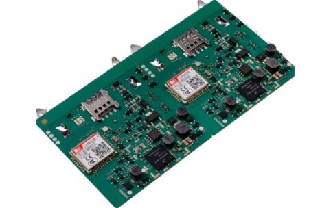
The automotive high power PCB market is expected to hit $2.8 billion in 2026, growing at an 11.4% CAGR through 2035. 800V fast-charging platforms and on-board chargers (OBC) require PCBs that carry 50A+ currents, withstand 1000V+ voltages and maintain stability across -40℃ to 85℃ outdoor temperature cycles. EV charger PCBA, in particular, demands integrated EMC filtering, leakage protection and heavy copper power paths — all of which depend on precision-controlled PCB and PCB assembly services.
1.2 Grid-Tied Energy Storage & Renewable Inverters
Global renewable energy installations continue to expand, with nearly 47% of heavy copper PCB demand coming from power conversion systems for solar, wind and battery energy storage. Bi-directional energy storage converters operate at high voltage and high current for 24/7 duty cycles, requiring PCB designs with symmetrical stack-up, low thermal resistance and long-term anti-aging performance.
1.3 Industrial & Server Power Supplies
The EU’s 2025/1399 Ecodesign Directive mandates minimum 94% efficiency (80 PLUS Titanium) for power supplies above 250W starting in 2026, forcing OEMs to upgrade from silicon MOSFETs to GaN-based topologies. Higher switching frequencies (1MHz+) introduce stricter requirements for parasitic inductance control in PCB layout and assembly, making poorly optimized boards prone to voltage overshoot, EMI failure and premature component breakdown.
1.4 AI Data Center Power Distribution
AI server clusters demand high-current, high-reliability power distribution boards with tight voltage regulation. The surge in AI infrastructure has extended lead times for specialty high-performance laminates to 12–16 weeks, creating supply chain uncertainty for power supply OEMs that rely on multi-vendor sourcing models.
2. Key Procurement Pain Points for High Power PCBA in 2026
Industry surveys of power supply OEM procurement managers show that technical and supply chain risks remain the top concerns in 2026, most of which stem from fragmented or under-qualified PCB and PCB assembly services:
2.1 SiC/GaN Layout Complexity Causing Design Iteration Delays
SiC MOSFETs switch at dV/dt rates above 50V/ns, and even 20nH of stray power loop inductance can generate 40V of overshoot on a 400V DC bus — enough to destroy devices at full load. Many PCB vendors lack WBG-specific layout experience, resulting in multiple design spins, delayed certification and missed market windows. A 2026 industry report notes that 62% of power supply NPI delays are caused by suboptimal PCB layout for SiC/GaN circuits.
2.2 Thermal Failure Remains the #1 Field Reliability Risk
Over 55% of high power supply field failures trace back to thermal imbalance and poor heat dissipation in PCB and PCBA construction. Low-Tg FR4 substrates, thin copper foils and insufficient thermal vias cause localized hotspots, substrate delamination and solder joint cracking under thermal cycling. For outdoor EV chargers and industrial inverters, each 10℃ rise in operating temperature cuts component service life in half, driving up warranty and on-site maintenance costs.
2.3 Stricter Global Compliance & Certification Standards
CE, UL and IEC 61851 certification bodies are tightening creepage distance, EMC and thermal safety requirements for high-power equipment in 2026. OEMs working with suppliers that lack familiarity with regional safety standards often face batch rejections at certification labs, resulting in 8+ week launch delays and six-figure rework costs.
2.4 Split Supply Chain Creates Accountability Gaps
Most buyers still source bare PCBs from one vendor and assembly services from another. When thermal or electrical failures occur, the PCB fabricator blames the assembly house and vice versa — leaving the OEM to absorb the loss. This fragmented model also makes it nearly impossible to implement unified thermal process control across fabrication and assembly.
2.5 Material Volatility & Unpredictable Lead Times
Copper price fluctuations and specialty laminate shortages continue to disrupt production schedules in 2026. Small-scale suppliers without safety stock or alternate material qualification capabilities frequently push out delivery dates or force unvalidated material substitutions that compromise reliability.
3. How Professional PCB and PCB Assembly Services Solve 2026 Power Supply Challenges
Integrated PCB and PCB assembly services unify design, fabrication, component sourcing and testing under one quality management system, directly addressing the pain points above. For high power supply applications, the value is delivered across four critical stages:
3.1 DFM-Forward Design Optimization for WBG & High Power Topologies
Expert PCB and PCB assembly services begin with design for manufacturability (DFM) review before fabrication starts. For SiC and GaN power circuits, this includes:
- Minimizing power loop and gate loop area to reduce parasitic inductance
- Optimizing heavy copper trace geometry for uniform current distribution
- Placing dense thermal via arrays under power devices to lower junction temperature
- Defining proper creepage and clearance distances to meet high-voltage safety standards
- Simulating thermal performance to identify hotspots before board production
This upfront optimization reduces NPI iterations by 40–60% and dramatically lowers certification failure risk.
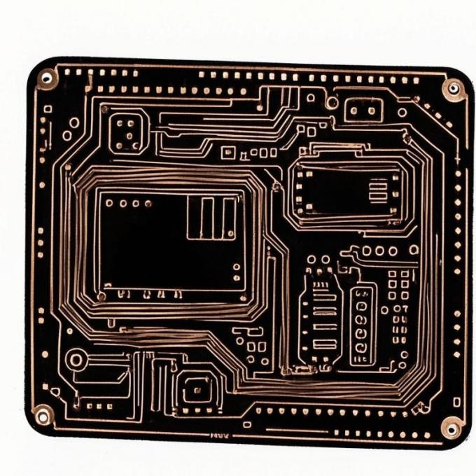
3.2 Precision Heavy Copper & High-Tg PCB Fabrication
High power performance starts with the bare board. Qualified PCB and PCB assembly services offer specialized fabrication capabilities:
- Heavy copper construction: 2oz to 10oz copper weights for high-current paths, reducing I²R losses and improving heat spreading
- High-Tg & thermally conductive substrates: 170℃+ Tg FR4, metal core PCB (MCPCB) and ceramic substrates for extreme thermal environments
- Filled & capped thermal vias: Epoxy-filled vias eliminate air gaps and improve vertical heat transfer by 30–40%
- Symmetric stack-up design: Controls board warpage under thermal cycling and ensures uniform contact with heat sinks
The global heavy copper PCB market is expected to reach $2.71 billion in 2026, reflecting how critical this capability has become for power supply OEMs.
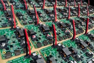
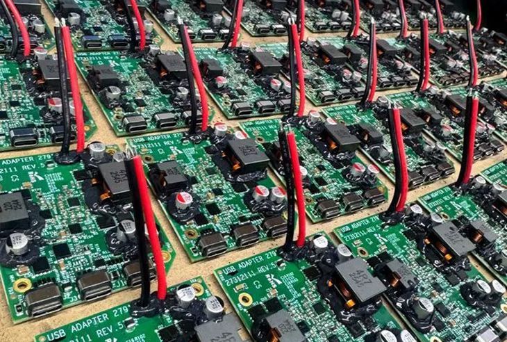
3.3 Controlled Assembly Processes for High-Reliability Solder Joints
Even the best PCB design fails with poor assembly. Professional PCB and PCB assembly services implement power-specific assembly controls:
- Customized reflow temperature profiles calibrated for heavy copper boards and high-temperature components
- Solder void ratio control below 5% for power device thermal pads (industry average can exceed 35% with unoptimized processes)
- Precision application of thermal interface materials (TIM) to ensure consistent heat transfer
- Automated first article inspection (FAI) verifying component polarity, placement accuracy and BOM consistency before mass production
- Selective soldering for through-hole power components to avoid thermal damage to sensitive devices
3.4 Multi-Dimensional Reliability Validation
Reliability cannot be assumed — it must be tested. Mature PCB and PCB assembly services include mandatory reliability verification for high-power products:
- Thermal cycling testing (-40℃ ~ 85℃) to validate solder joint and substrate integrity
- Infrared thermal imaging under full load to identify hidden hotspots
- 24-hour continuous burn-in testing at rated power
- High voltage insulation and Hi-Pot testing for safety compliance
- Humidity and temperature bias (HTHB) testing for outdoor-rated products
Full test reports accompany every shipment, supporting customer certification submissions and third-party factory audits.
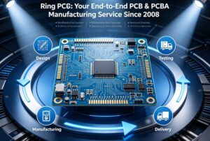
4. RingPCB: Your Trusted Source Factory for High Power PCB and PCB Assembly Services
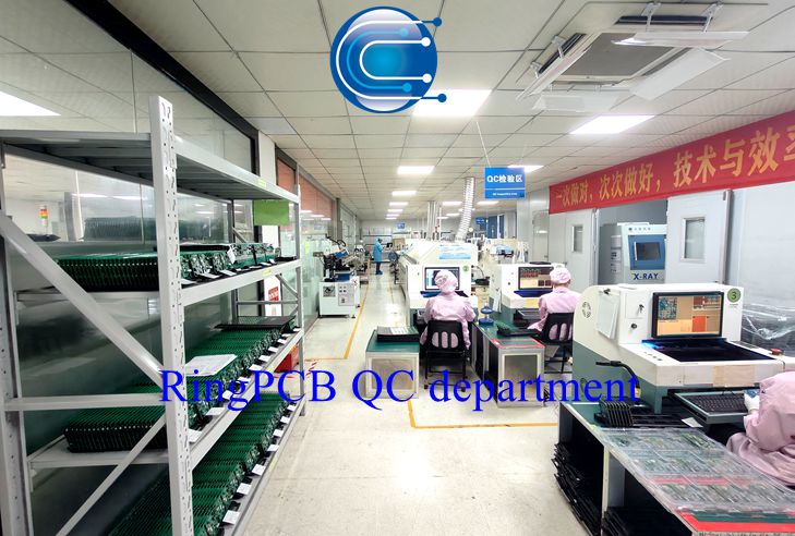
As an ISO 9001, IATF 16949 and UL certified one-stop PCB & PCBA manufacturer founded in 2008, RingPCB specializes in high-reliability PCB and PCB assembly services tailored for power supply applications. Our 10,000㎡ in-house automated factory combines bare PCB fabrication, authorized component sourcing, SMT/DIP assembly and full reliability testing under a single quality system — eliminating split-supply-chain accountability gaps.
4.1 Technical Capabilities Tailored for High Power Systems
- Heavy copper PCB production: 2–10oz copper weight with precision etching and controlled warpage (≤0.5%)
- WBG design expertise: In-house engineering team with SiC/GaN layout experience, providing free DFM and thermal simulation review for every project
- Advanced material portfolio: High-Tg FR4, aluminum MCPCB, ceramic substrates and copper-inlaid structures
- IPC-A-610 Class 3 assembly: Strict process controls achieving <3% void rate on power device thermal pads
- Comprehensive in-house testing: Thermal cycling, IR thermography, Hi-Pot, AOI, X-ray and functional burn-in
4.2 Overcoming Key Technical Challenges
RingPCB has solved long-standing pain points that plague many power supply OEMs:
- Thermal runaway risk: Our DFM team optimizes copper pour, thermal via placement and component layout to reduce peak component temperatures by 20–30℃
- EMI certification failure: EMC-aware layout and controlled impedance routing help customers pass CE/FCC testing on the first attempt
- Heavy copper warpage: Proprietary sequential lamination and symmetric stack-up technology eliminates assembly-level warpage issues that cause poor heat sink contact
- Supply chain uncertainty: Strategic safety stock of common high-power laminates and long-term agreements with authorized component distributors stabilize lead times and pricing
4.3 End-to-End Service Benefits for Power Supply OEMs
- Single point of contact: One engineering and project management team owns the entire project from Gerber to finished PCBA
- Faster NPI: Integrated design, fabrication and assembly cuts prototype lead times by 30% compared to multi-vendor workflows
- Lower total cost: Upfront DFM optimization reduces rework, field failures and warranty expenses over the product lifecycle
- Flexible order volumes: Support from 1-piece prototype validation to 100,000+ unit monthly mass production
- Full traceability: MES system records all material batches, process parameters and test data, ready for customer and regulatory audits
4.4 Real-World Result: 7kW EV Charger PCBA Reliability Upgrade
A European EV charger OEM switched to RingPCB’s PCB and PCB assembly services after experiencing 12% field failure rate from thermal overstress. Our team upgraded the design from 2oz to 4oz heavy copper high-Tg PCB, added optimized thermal via arrays under power MOSFETs, and calibrated the reflow profile to cut thermal pad voids from 38% to 3.2%. After mass deployment, the customer’s field failure rate dropped to 0.18%, reducing annual after-sales costs by over $180,000.
5. Looking Ahead: 2026–2027 Technology Trends
The evolution of high power supply systems will continue to push PCB and PCB assembly services toward higher integration and intelligence:
- Embedded power PCB technology: 2026 is a critical year for SiC chip embedding into PCB substrates, enabling 3D interconnection that eliminates bond wires and boosts thermal performance
- Hybrid substrate architectures: Mixed FR4/ceramic/metal core boards will balance cost and thermal performance for medium-power applications
- AI-assisted quality inspection: AI-powered AOI and X-ray systems will detect micro-defects in heavy copper solder joints with higher accuracy
- Sustainability requirements: Rising regulatory focus on product lifespan and recyclability will favor suppliers with proven long-term reliability capabilities
Conclusion
In 2026, high power supply systems are more capable — and more demanding — than ever before. Success depends not just on component selection, but on choosing a partner that delivers fully optimized, quality-controlled PCB and PCB assembly services from design through testing. The right source factory partner reduces thermal failure risks, speeds certification, stabilizes supply chains and lowers total ownership cost.
RingPCB’s dedicated power electronics division delivers exactly that: end-to-end PCB and PCB assembly services built for the thermal, electrical and reliability demands of modern high power supplies. Whether you are developing EV charger PCBA, energy storage inverters, industrial power supplies or server PSU boards, our engineering team will optimize your design for manufacturability, thermal performance and long-term reliability.
Send your Gerber files and BOM to rfq@ringpcb.com for a free DFM review and custom quotation, or visit www.ringpcb.com to explore our full range of high power PCB and PCBA capabilities.