1. Core Procurement Pain Points Brought by Unqualified PCB and PCB Assembly Services
- Hidden thermal design defects trigger batch rejection in overseas certification
Many small PCB factories lack professional thermal simulation engineers, leaving power MOSFET, IGBT and transformer zones without sufficient thermal vias or heavy copper pour. One EV charger OEM shared that their previous supplier’s standard PCB and PCB assembly services ignored IEC 61851 creepage and thermal layout rules, resulting in the entire 5,000-unit production batch failing CE EMC thermal testing, causing 8 weeks of production delay and $120,000 rework losses.
- Unstable thermal reliability raises long-term after-sales costs
Industry data confirms that every 10℃ rise in PCB operating temperature halves electronic component service life. Cheap PCB and PCB assembly services using low-Tg substrates will see PCB delamination after only 500 thermal cycles, pushing annual equipment failure rates above 15%. For 7kW residential EV chargers, each on-site maintenance costs roughly $43; unoptimized thermal PCBA solutions add up to $2,150 extra maintenance expenses per unit over a 5-year service cycle.
- Separated PCB fabrication and PCBA assembly suppliers create thermal coordination gaps
Most buyers split orders between separate PCB manufacturers and assembly factories, with no unified thermal design standard. Layout mismatch, inconsistent reflow temperature curves and unregulated thermal interface material application create invisible heat bottlenecks that neither supplier takes responsibility for. RingPCB’s integrated PCB and PCB assembly services eliminate this split supply chain flaw as a self-owned source factory.
- Lack of customized thermal processing options for high power density demands
Modern high power supply systems (such as 22kW EV charger PCBA, bidirectional energy storage converters) reach thermal flux density up to 15W/cm², requiring heavy copper PCB, metal core PCB and filled thermal via technology. General small factories cannot support 2–10oz heavy copper etching, conformal coating or thermal cycling aging testing, forcing buyers to compromise on thermal performance.
2. How Standardized PCB and PCB Assembly Services Fix Thermal Bottlenecks for High Power Supplies
2.1 Thermal optimization at PCB design & DFM stage
- Heavy copper trace & power plane layout: We customize 3oz–8oz thick copper circuits for high-current paths, reducing local temperature rise by 20–30℃ compared to standard 1oz copper boards. For 50A+ power modules, we adopt copper embedding technology to lower trace thermal resistance by 42%.
- Dense thermal via array design: Under all high-power heat-generating components, we arrange 0.3mm filled thermal vias at a density of 25 vias per square centimeter, building vertical heat conduction channels to inner ground planes, strictly following IPC-2152 current-carrying and thermal layout standards.
- Hotspot zoning separation: Our DFM engineers isolate power heating zones from sensitive capacitors and signal chips with 5mm clearance, avoiding thermal crosstalk that drifts circuit sampling accuracy.
2.2 High-spec bare PCB manufacturing to lock in thermal base performance
- High-Tg thermal-resistant substrate matching: For outdoor EV charger PCBA and industrial power boards, we exclusively adopt 170℃+ high-Tg FR4, aluminum metal core PCB and ceramic substrates instead of cheap ordinary FR4. Standard FR4 only delivers 0.3W/m·K thermal conductivity, while our MCPCB reaches 80W/m·K, cutting component junction temperature by up to 40℃.
- Symmetric stack-up & controlled warpage technology: Heavy copper PCB easily generates severe board warpage under repeated thermal cycling, breaking solder joints during assembly. RingPCB adopts sequential lamination and symmetric copper balance processes, controlling finished board warpage below 0.5% to guarantee uniform thermal contact with heat sinks.
- Insulated filled thermal via process: Conventional hollow vias trap air and raise thermal resistance; our proprietary epoxy-filled via technology eliminates air gaps, stabilizing long-term heat transfer efficiency even after thousands of charge-discharge cycles.
2.3 Rigorous PCBA assembly thermal process & full reliability testing
- Customized reflow temperature curves for heavy copper boards: Thick copper absorbs far more heat than standard boards; generic reflow profiles cause insufficient solder wetting or overheating substrate degradation. Our equipment automatically adjusts heating ramp rates according to board copper thickness, ensuring void ratio under power device thermal pads stays below 5% (industry average void rate reaches 35% for unqualified assembly).
- Regulated thermal interface material (TIM) application: We precisely control TIM thickness and coating area for all power components mounted to heat sinks, avoiding uneven contact resistance that creates hidden hotspots during continuous high-load operation.
- Multi-dimensional thermal reliability testing as mandatory delivery standard
Every batch of finished PCBA from RingPCB’s PCB and PCB assembly services passes 4 layers of thermal verification before shipment:
- Infrared thermal imaging full-load temperature scanning to locate hidden hotspots
- -40℃ ~ 85℃ thermal cycling test with 2,000 cycles to simulate extreme seasonal environments
- 24-hour full-load aging test under maximum rated power to record continuous temperature drift data
- High-temperature 85℃/85%RH humidity heat test to verify substrate and solder joint anti-aging performance
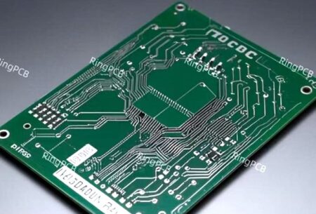
3. RingPCB Source Factory: Differentiated PCB and PCB Assembly Services for High Power Supply Thermal Demands
- Full industrial certification system for high-power thermal PCBA
We hold ISO 9001, IATF 16949, ISO 14001 and UL certifications, fully compliant with IEC 61851 (EV charging), IEC 62368-1 (industrial power supply) and IPC-A-610 Class 3 high-reliability standards. Our PCB and PCB assembly services fully meet thermal safety requirements for new energy, automotive and industrial high-power equipment exports to EU, North America and Southeast Asia markets.
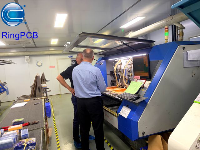
- Independent automated production lines for heavy copper & thermal PCB manufacturing
Our factory operates dedicated production workshops for 2–10oz heavy copper PCB and metal core PCB, equipped with automatic thermal simulation pre-production inspection equipment, automated FAI first-piece inspection systems and infrared thermal imaging testing stations. We have independently solved the technical bottleneck of heavy copper uneven etching and board warpage, supporting mass production of high thermal performance EV charger PCBA, industrial power PCBA and energy storage circuit boards.
- Full turnkey service to eliminate cross-supplier thermal coordination risks
Unlike suppliers that only provide single PCB fabrication or assembly, RingPCB’s all-in-one PCB and PCB assembly services unify thermal design, substrate production, component welding and reliability testing under one factory. Our dedicated thermal engineering team tracks every project from Gerber file review to after-delivery technical support, taking full responsibility for all thermal performance issues, completely removing the blame-shifting problems of split supply chains.
- Flexible order capacity for prototype to mass thermal PCBA
We support small-batch thermal prototype customization (1–50 pieces) for new product NPI thermal verification, as well as large-volume mass production up to 100,000 units monthly. Our stable franchised component supply channels source industrial-grade high-temperature power chips, capacitors and inductors, avoiding low-grade components that accelerate thermal aging and reduce board lifespan.
- Free thermal DFM review & customized thermal processing add-ons
All customers receive complimentary thermal layout optimization during the quotation phase of our PCB and PCB assembly services. Optional value-added thermal treatments include acrylic/silicone conformal coating, copper inlay heat spreading structures and custom thermal pad opening designs, extending the service life of outdoor high-power supply PCBA by over 5 years.
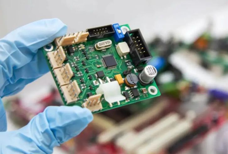
4. Real Case: Thermal Stability Upgrade for 7kW EV Charger PCBA via RingPCB’s PCB and PCB Assembly Services
- Upgraded original 2oz copper PCB to 4oz heavy copper high-Tg substrate, adding 32 thermal vias under each power MOSFET;
- Rearranged component layout to separate the EMC filter heating zone from control signal circuits;
- Adjusted SMT reflow curve to reduce thermal pad void rate from 38% to 3.2%;
- Conducted 2,000-cycle thermal cycling and 24-hour full-load aging testing for all finished EV charger PCBA.