In 2026, the global communication industry is driven by the large-scale commercial rollout of 5G-A, mass shipment of 1.6T optical modules, and pre-research layout of 6G millimeter wave systems, which completely rewrite the evaluation standards of high performance PCB manufacturing for communication. A high-performance communication PCB is no longer a simple circuit carrier; it is the core hardware foundation that determines signal transmission efficiency, equipment stability and long-term operation reliability. Every link of high performance PCB manufacturing for communication, including material matching, precision fabrication, signal integrity testing and reliability verification, directly restricts the commercial progress of base stations, data center switches and optical communication devices. Industry data shows that the 2026 communication PCB market will reach 35.25 billion RMB, with high-frequency high-speed high performance PCB products accounting for more than 52% of the total market demand, and the market growth rate of high performance PCB manufacturing for communication will stay at 10% year-on-year. For electronics manufacturers and EMS service providers, mastering the core logic of high performance PCB manufacturing for communication has become a necessary condition to enter the supply chain of mainstream communication brands.
1. High-performance Material Matching: The Foundation of Qualified Communication PCB Manufacturing
The first core of high performance PCB manufacturing for communication lies in scientific and customized substrate matching, which is the primary premise to guarantee low signal loss under high frequency and high speed conditions. Traditional FR-4 ordinary substrates cannot meet the transmission demand of 224Gbps PAM4 signals on 1.6T optical modules, so professional high performance PCB manufacturing for communication must deploy diversified low-loss high-frequency materials as standard configuration. At present, mainstream materials adopted in mature high performance PCB manufacturing for communication include Rogers series PTFE substrates, Panasonic Megtron 6/7 hydrocarbon plates and domestic modified PPO high-speed copper clad laminates, whose Df loss factor can be controlled below 0.002 at 10GHz to avoid serious signal attenuation of millimeter wave communication equipment.
In high performance PCB manufacturing for communication, manufacturers need to design hybrid stacking schemes according to customer equipment scenarios: using ultra-smooth HVLP copper foil for high-frequency signal layers to reduce skin effect loss, while adopting conventional copper foil for power supply layers to balance production cost and performance. This targeted material collocation is an important dividing line between general PCB factories and manufacturers specializing in high performance PCB manufacturing for communication. Many small-scale factories only stock single ordinary substrates, which leads to unstable impedance and high insertion loss of finished communication boards, resulting in batch rejection after customer testing.
In addition to core copper clad laminates, auxiliary materials such as prepreg and surface treatment materials also affect the overall performance of communication PCB in high performance PCB manufacturing for communication. For millimeter wave base station PCBs, ENIG chemical nickel gold surface treatment is mandatory to maintain stable contact resistance in high-frequency transmission; mass production of high performance PCB manufacturing for communication must strictly control the gold thickness between 0.05–0.1μm to prevent signal reflection caused by uneven surface coating. Material incoming IQC inspection runs through the whole high performance PCB manufacturing for communication process, and each batch of substrates needs to provide Dk/Df test reports to ensure batch consistency of finished circuit boards.
2. Advanced Fabrication Process: The Technical Core of High Performance Communication PCB Manufacturing
Process precision control is the second indispensable core of high performance PCB manufacturing for communication, and 2026’s mainstream high-speed communication equipment has completely eliminated the traditional subtractive etching process, taking mSAP modified semi-additive process as the standard production route. Compared with ordinary processes, mature high performance PCB manufacturing for communication relying on mSAP technology can realize ultra-fine line width/spacing of 15–40μm, and control impedance tolerance within ±2%, fully matching the wiring density demand of 1.6T and 3.2T optical module PCBs. Traditional subtractive process can only achieve 75μm line width at minimum, which cannot support the miniaturization and high integration trend of new generation communication hardware.
Laser Direct Imaging (LDI) and UV laser microvia drilling are standard equipment configurations for professional high performance PCB manufacturing for communication. In 5G-A small cell millimeter wave PCBs, the minimum blind via diameter is required to reach 50μm, and only composite laser drilling equipment can ensure smooth hole walls without glass fiber burrs, avoiding open circuits and unstable interlayer signals after lamination. Layer alignment accuracy is another key process index of high performance PCB manufacturing for communication: top-tier manufacturers control interlayer registration error within 75μm through automatic optical alignment equipment, while backward factories have alignment deviation exceeding 120μm, which directly changes dielectric thickness and breaks impedance matching design.
Thermal process control such as vacuum lamination and plasma desmear also decides the yield of high performance PCB manufacturing for communication. Communication high-multilayer PCBs above 24 layers are prone to interlayer bubbles and delamination under conventional hot pressing; vacuum lamination equipment used in standardized high performance PCB manufacturing for communication eliminates air gaps between layers, and passes 20 times thermal shock testing without stratification, meeting IPC-6012 Class 3 industrial communication standards. Plasma desmear technology thoroughly removes resin residues in microvias, ensuring stable conductivity of interconnection holes, which effectively reduces the failure rate of communication PCB in long-term high-temperature operation.
3. Strict Signal Integrity & Reliability Testing: Quality Guarantee of High Performance Communication PCB Manufacturing
Complete testing systems form the third core barrier of high performance PCB manufacturing for communication, distinguishing qualified high-performance communication circuit boards from ordinary products. Unlike consumer electronics PCB that only conduct simple open-short testing, high performance PCB manufacturing for communication must carry out full-link signal integrity testing covering impedance scanning, insertion loss detection, crosstalk simulation and thermal cycling aging verification before delivery. For optical communication high-speed boards working at 56GHz, each panel needs full-length insertion loss scanning to ensure the loss per inch is lower than 1.5dB, otherwise high-speed data transmission will generate serious delay and bit error rate rise.
Reliability aging testing is a non-negotiable link in high performance PCB manufacturing for communication, targeting the complex operating environment of outdoor base stations and data center equipment. Standard test items include -40℃~125℃ temperature cycling test, high temperature and humidity storage test, salt spray corrosion test and thermal stress test after reflow soldering. Communication PCBs produced by factories without complete testing links often appear pad peeling and circuit fracture after 3–6 months of field operation, bringing huge maintenance losses to communication equipment brands.
In standardized high performance PCB manufacturing for communication, all test data of each circuit board will be archived by batch and serial number to realize full traceability. When customers encounter signal problems after assembly, manufacturers can quickly locate abnormal links from substrate batch, process parameters to testing records. This traceability system is an important service advantage of professional suppliers in high performance PCB manufacturing for communication, and it is also an important assessment index for communication OEMs to screen qualified PCB partners.
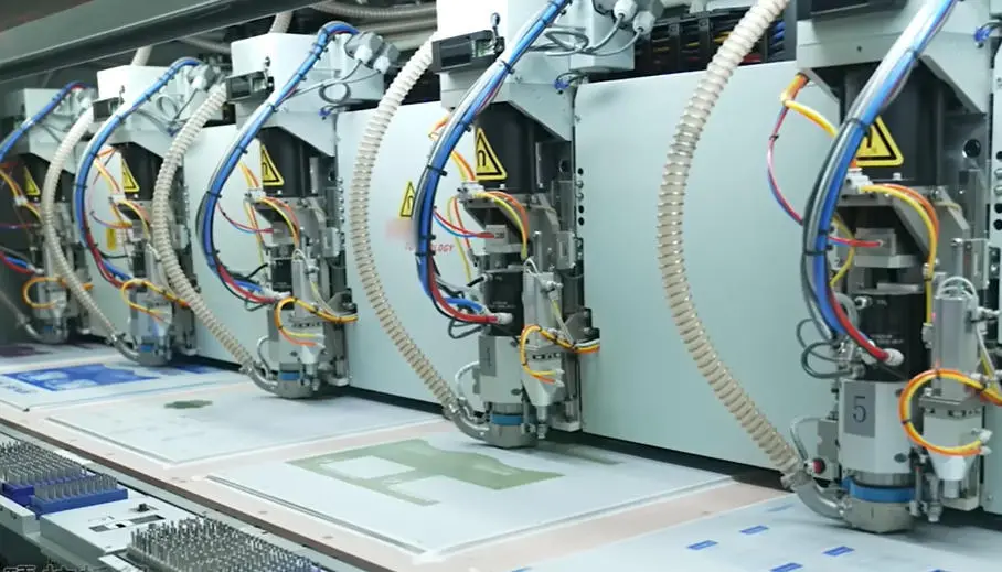
4. Intelligent Digital Production: New Core Competitiveness of 2026 Communication PCB Manufacturing
2026 ushers in the digital intelligent transformation stage of high performance PCB manufacturing for communication, and digital twin production lines have become the new core competitiveness of leading manufacturers. Traditional production relying on manual parameter adjustment cannot cope with the strict precision requirements of millimeter wave and ultra-high-speed communication PCBs, while intelligent workshops deploy thousands of real-time sensors to monitor 150+ process parameters such as lamination temperature, laser energy and etching liquid concentration, and dynamically adjust production parameters through AI algorithms. Data shows that after deploying intelligent control systems in high performance PCB manufacturing for communication, impedance qualification rate rises from 92% to 98.5%, and production rework rate drops by more than 60%, greatly improving delivery efficiency for mass communication PCB orders.
Intelligent MES management system runs through the whole high performance PCB manufacturing for communication process, realizing automatic tracking from Gerber file receiving, DFM compliance review, material feeding, each process production to finished product testing and packaging. Before formal production, the engineering team completes professional DFC design compliance review aiming at communication signal characteristics, pre-judging hidden risks such as unreasonable stack-up, insufficient isolation of differential pairs and mismatched dielectric thickness, avoiding mass scrapping caused by design defects after production starts. This front-end intelligent review mechanism greatly optimizes the overall cycle of high performance PCB manufacturing for communication, shortening prototype delivery time to 3 working days.
Supply chain digital synchronization is also an important part of intelligent high performance PCB manufacturing for communication. Professional communication PCB manufacturers establish long-term cooperative relations with global high-frequency substrate suppliers, and realize real-time synchronization of material inventory through digital platforms, solving the industry-wide shortage of high-speed copper clad laminate in 2026. Small factories without digital supply chain management often face material out-of-stock, resulting in delayed delivery of customer communication equipment projects.
5. End-to-End Turnkey Manufacturing: Integrated Core Advantage to Lower Customer Comprehensive Costs
The ultimate core value of mature high performance PCB manufacturing for communication lies in integrated full-turnkey one-stop service, covering PCB fabrication, authorized component sourcing, SMT/DIP assembly and finished PCBA function testing. Most communication brand customers used to cooperate with separate PCB factories and assembly manufacturers, resulting in disconnection of process standards and unclear responsibility division when signal quality problems occur. Integrated high performance PCB manufacturing for communication providers unify all links under one quality management system, with a single team responsible for all performance and delivery issues of communication circuit boards.
For communication equipment purchasers, choosing suppliers with integrated high performance PCB manufacturing for communication capability can greatly reduce procurement communication costs and supply chain risks. The supplier completes material certification, impedance testing, SMT high-precision welding and X-Ray void inspection of BGA chips independently, and delivers finished communication PCBA products that can be directly installed into equipment. This one-stop model is widely favored by 5G base station manufacturers, optical module enterprises and data center switch brands in 2026, and becomes the mainstream cooperation mode of high performance PCB manufacturing for communication.
Conclusion
The core of high performance PCB manufacturing for communication in 2026 revolves around four key dimensions: high-frequency low-loss material matching, ultra-precision advanced fabrication processes, full-coverage signal integrity reliability testing and digital intelligent production management, while integrated end-to-end turnkey service further amplifies the comprehensive value of communication PCB manufacturing. With the continuous acceleration of 5G-A commercialization and 1.6T optical module mass production, the market threshold of high performance PCB manufacturing for communication will keep rising, and only manufacturers with complete certifications, advanced production equipment and mature communication project experience can stably meet global brand demands.
If you are looking for a reliable supplier of high performance PCB manufacturing for communication, RingPCB, founded in 2008, owns a 10,000㎡ self-operated automated factory specializing in communication high-frequency high-speed PCB and full turnkey PCBA manufacturing. We hold ISO9001, IATF16949, ISO14001, ISO13485 and UL full certifications, support mSAP ultra-fine line process, millimeter wave high-frequency board customization, rapid 3-day prototype and mass production delivery for optical modules, 5G small cells and data center communication equipment. Send your Gerber files, BOM and communication project requirements to rfq@ringpcb.com for free DFM review and customized quotation. Visit our official website https://www.ringpcb.com to check our communication PCB manufacturing cases, factory production equipment and complete qualification documents.