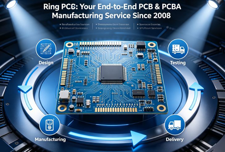
Introduction
1. Verify Complete Industry Certifications Tailored for Communication PCB Projects
Without these targeted credentials, the circuit boards produced cannot pass overseas customs inspection and third-party communication equipment performance testing. Formal partner of PCB manufacturing and assembly for communication will archive all certification files and provide them to customers for free DFM audit at the prototype stage, which effectively eliminates compliance risks for cross-border communication brands.
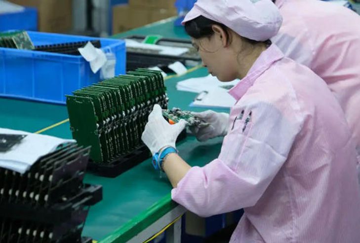
2. Inspect Production Processes & Equipment for High-Speed Communication Circuit Boards
In 2026, mainstream communication hardware requires 15–40μm ultra-fine wiring and ±2% impedance tolerance; only standardized partner of PCB manufacturing and assembly for communication with full vacuum lamination and plasma desmear machines can control interlayer alignment errors within 75μm. You can request factory video tours or on-site audits to check the operation status of high-frequency PCB dedicated production lines of your potential partner of PCB manufacturing and assembly for communication, to avoid suppliers outsourcing communication board orders to small foundries with backward processes.
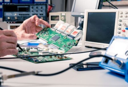
3. Audit Full Signal Integrity & Reliability Testing Capacity
Communication high-speed boards operate under high-frequency and high-temperature conditions for a long time; the partner of PCB manufacturing and assembly for communication needs to finish full signal integrity scanning and multi-cycle reliability aging before delivery. Reputable partner of PCB manufacturing and assembly for communication can provide batch test reports with serial number traceability, which helps customers quickly locate abnormal signal faults after PCBA assembly and equipment assembly. Suppliers lacking independent testing workshops will lead to high defective rates of finished communication products, raising after-sales labor and material costs.
4. Evaluate Turnkey PCBA One-Stop Service Capability
This full turnkey mode greatly reduces communication costs for communication purchasers, and the partner of PCB manufacturing and assembly for communication delivers finished communication PCBA that can be directly installed into base stations, optical transceivers and switches. In 2026, more than 70% medium and large communication enterprises prefer one-stop partner of PCB manufacturing and assembly for communication to simplify their global supply chain layout and reduce inventory pressure.
5. Assess Flexible MOQ, Delivery Cycle & Technical After-Sales Support
In addition, the technical team of the partner of PCB manufacturing and assembly for communication should offer free DFM design review before production, proactively optimizing stack-up, differential pair layout and grounding structure to reduce signal attenuation risks. Timely after-sales response mechanism is also essential: formal partner of PCB manufacturing and assembly for communication arranges dedicated project managers to track every communication PCB order, solving technical and quality problems within 24 hours to prevent project schedule delays.