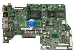
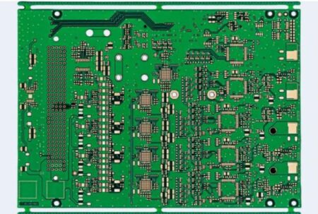
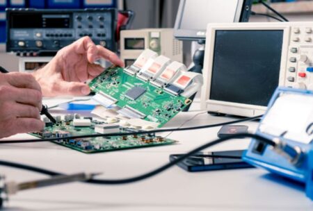
A Multilayer High Frequency PCB is a precision-engineered printed circuit board designed for RF, microwave, and high-speed digital applications operating above 1GHz.
Unlike standard FR-4 boards, high frequency PCBs require low-loss dielectric materials, strict impedance control, and highly stable multilayer structures to ensure reliable signal transmission.
Ring PCB specializes in OEM Multilayer High Frequency PCB manufacturing, delivering customized RF PCB solutions for 5G infrastructure, automotive radar systems, satellite communications, and advanced networking equipment.
Key Features of Ring PCB Multilayer High Frequency PCB
Ring PCB designs and manufactures high-performance Multilayer High Frequency PCBs with strict process control and OEM flexibility.
Core product advantages include:
- OEM / ODM customization for RF applications
- Up to 48-layer multilayer PCB capability
- Controlled impedance accuracy up to ±7%
- Low-loss high-frequency material selection
- Fast prototyping and scalable mass production
- RF engineering and stack-up design support
With ISO9001, ISO14001, ISO13485, and IATF16949 certifications, Ring PCB ensures stable quality across industrial, automotive, and medical-grade applications.
Real Application Cases of Multilayer High Frequency PCB
Case 1: 5G Base Station RF Module (Telecom Industry)
A European telecom equipment manufacturer required a low-loss multilayer PCB for a 5G base station RF module operating in high-frequency bands.
Challenge:
- Signal attenuation above 3GHz
- Impedance instability in multilayer design
- Thermal reliability under continuous load
Ring PCB Solution:
- Rogers RO4350B + hybrid RF stack-up design
- ±7% impedance controlled manufacturing
- Optimized multilayer alignment process
Result:
Stable RF signal transmission with significantly reduced insertion loss, supporting continuous high-load 5G operation.
Case 2: Automotive Radar System PCB (ADAS Application)

An automotive Tier-1 supplier required a high-frequency PCB for 77GHz radar sensing systems used in ADAS (Advanced Driver Assistance Systems).
Challenge:
- Extremely tight tolerance requirements
- High-frequency signal integrity under vibration
- Multi-layer alignment precision
Ring PCB Solution:
- PTFE-based low-loss materials
- Laser drilling via precision control
- High-accuracy lamination process
Result:
Improved radar detection accuracy and stable performance in automotive environments.
Case 3: Satellite Communication Equipment PCB
A satellite communication system integrator needed a multilayer RF PCB for signal transmission modules used in space communication equipment.
Challenge:
- Low dielectric loss requirement
- High reliability in extreme environments
- Long-term signal stability
Ring PCB Solution:
- Rogers RF-grade laminates
- Enhanced copper surface treatment
- Strict AOI + X-ray inspection process
Result:
Stable signal integrity under long-duration satellite operation conditions.
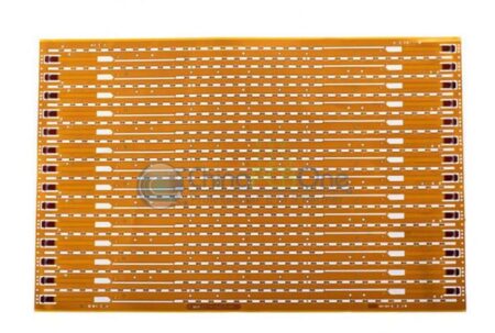
Materials Used in Multilayer High Frequency PCB
Material selection plays a critical role in RF PCB performance.
Ring PCB uses advanced materials including:
- Rogers RO4003C / RO4350B
- Taconic RF laminates
- PTFE-based substrates
- Hybrid FR-4 + RF stack-up materials
Compared with standard FR-4, these materials provide:
- Lower dielectric loss
- Better high-frequency stability
- Reduced signal distortion
- Improved impedance consistency
Manufacturing Capability
Ring PCB supports advanced Multilayer High Frequency PCB production with:
- Layer count: 2–48 layers
- Line width/spacing: 3/3 mil
- Copper thickness: 0.5–3 oz
- Board thickness: 0.2–3.2 mm
- Impedance control: ±7%
- Surface finish: ENIG / OSP / Immersion Silver
- Assembly: SMT / THT / mixed technology
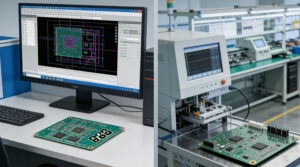
Manufacturing Process Overview
First, LDI imaging is used for high-precision circuit patterning.
Next, controlled etching defines accurate trace geometry.
Then multilayer lamination ensures precise alignment under strict temperature and pressure control.
After that, vias are formed using mechanical or laser drilling, followed by copper plating.
Finally, AOI and X-ray inspection ensure structural and electrical integrity.
Applications of Multilayer High Frequency PCB
Ring PCB Multilayer High Frequency PCBs are widely used in:
- 5G base station infrastructure
- RF transceiver modules
- Automotive radar systems (ADAS)
- Satellite communication systems
- Microwave communication devices
- High-speed networking systems
- Wireless and antenna systems
Technical Challenges & Engineering Support
High frequency PCB design involves several engineering challenges:
- Maintaining dielectric stability in multilayer structures
- Controlling impedance across RF signal paths
- Reducing surface roughness for signal loss reduction
- Ensuring via transition integrity
Ring PCB provides RF engineering support to optimize stack-up design and improve signal performance before production.
Technical Specifications
| Parameter | Capability |
|---|---|
| Layer Count | 2–48 layers |
| Impedance Control | ±7% |
| Line Width/Spacing | 3/3 mil |
| Copper Thickness | 0.5–3 oz |
| Board Thickness | 0.2–3.2 mm |
| Surface Finish | ENIG / OSP / Immersion Silver |
| Assembly Type | SMT / THT / Mixed |
FAQ
What is a Multilayer High Frequency PCB used for?
It is used in RF and microwave systems such as 5G communication, radar sensing, satellite transmission, and high-speed networking.
What industries use Ring PCB Multilayer High Frequency PCB?
It is widely used in telecommunications, automotive electronics, aerospace, and industrial RF systems.
Conclusion
Ring PCB Multilayer High Frequency PCB solutions are designed for high-performance RF and microwave applications where signal integrity, impedance control, and material stability are critical.
With proven applications in 5G infrastructure, automotive radar, and satellite communication systems, Ring PCB delivers reliable OEM manufacturing capabilities backed by advanced engineering and certified quality systems.