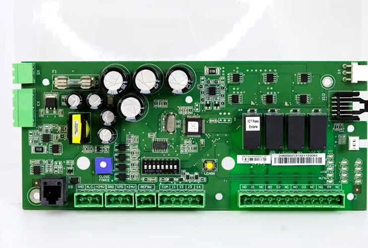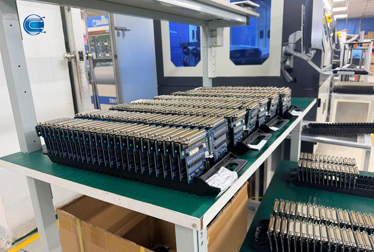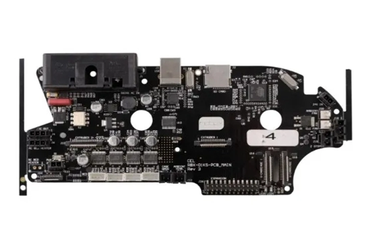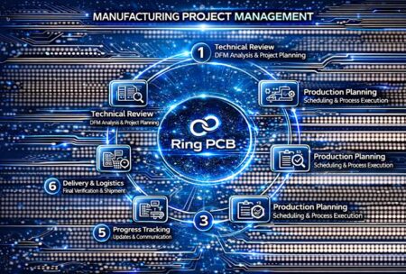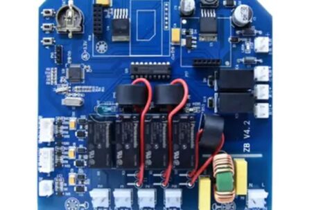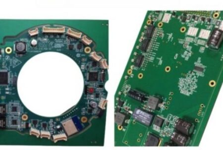
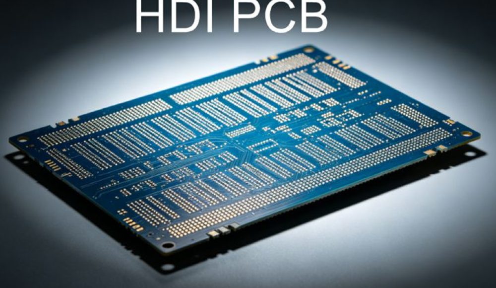
Modern electronic products continue to become smaller, faster, and more complex. Many engineers face challenges such as limited PCB space, signal integrity issues, and unreliable connections during high-density circuit design. HDI PCB technology provides a practical solution by using microvias, blind vias, and advanced layer structures to improve routing density and electrical performance. Ring PCB delivers HDI PCB manufacturing and turnkey assembly solutions from Shenzhen, China, helping global customers achieve reliable designs with strict quality control, fast production cycles, and professional engineering support.
Why Choose HDI PCB for Advanced Electronic Applications?
Traditional PCB designs often struggle when products require more components in a smaller footprint. High Density Interconnect PCB technology solves this challenge by increasing wiring density while maintaining signal reliability.
HDI PCBs use advanced manufacturing processes, including laser drilling and microvia technology, to create compact and efficient circuit structures.
Key advantages include:
- Compact PCB design: Microvias and blind/buried vias reduce board size and improve component placement flexibility.
- Improved signal integrity: Shorter signal paths reduce capacitance, inductance, and electromagnetic interference.
- Higher wiring density: Fine lines and smaller holes support complex circuits with high-pin-count components.
- Enhanced reliability: Advanced interconnect structures improve durability for demanding applications.
For example, an 8-layer conventional through-hole PCB can sometimes be redesigned into a 4-layer HDI PCB with similar functionality, reducing product size and weight.
Ring PCB HDI PCB Manufacturing Capabilities
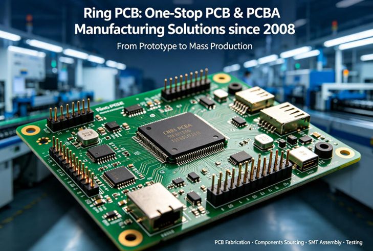
Ring PCB has provided PCB and PCBA solutions since 2008. Based in Shenzhen, China, the company operates a self-owned 10,000㎡ manufacturing facility with approximately 500 employees.
With 18 years of manufacturing experience, Ring PCB supports customers from rapid prototyping to volume production.
The company’s HDI PCB capabilities include:
- 2-48 layer PCB manufacturing
- FR4 HDI PCB fabrication
- Laser-drilled microvias
- Blind and buried vias
- High-density routing optimization
- SMT and through-hole assembly
- 100% AOI inspection and X-ray inspection
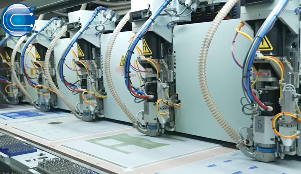
Ring PCB invests heavily in advanced production equipment, including:
- LDI laser exposure systems
- CNC drilling machines
- Vacuum lamination equipment
- High-speed SMT placement machines
- 8-stage lead-free reflow ovens
- Automated Optical Inspection (AOI)
- X-ray inspection systems
These capabilities allow Ring PCB to maintain stable lead times, with prototype production available within 3 days and mass production generally completed within 7 days.
HDI PCB Manufacturing Challenges and Ring PCB Solutions
| Manufacturing Challenge | Common Issue | Ring PCB Solution |
|---|---|---|
| Microvia drilling | Misalignment and electrical failures | High-precision laser drilling technology |
| Layer alignment | Signal problems caused by stacking errors | Automated alignment and precision lamination |
| Signal integrity | Crosstalk and signal loss | Impedance control and optimized PCB layout |
| Copper plating | Weak connections in microvias | Controlled copper deposition process |
| Quality inspection | Hidden manufacturing defects | AOI, X-ray inspection, and electrical testing |
By controlling every production stage internally, Ring PCB helps customers reduce manufacturing risks and maintain consistent PCB quality.
One-Stop HDI PCB Assembly and Manufacturing Process
When you choose Ring PCB as your HDI PCB manufacturer in China, you receive integrated PCB fabrication and assembly support.
The production process includes:
- Engineering review
- Analyze Gerber files, BOM data, and PCB requirements.
- Provide DFM/DFA optimization recommendations.
- PCB fabrication
- Complete material preparation, drilling, lamination, plating, and surface finishing.
- HDI structure production
- Manufacture microvias, blind vias, and high-density routing structures.
- Component assembly
- Complete component sourcing, SMT assembly, and through-hole assembly.
- Inspection and testing
- Perform AOI inspection, X-ray inspection, electrical testing, and functional verification.
- Delivery and support
- Provide reliable packaging, shipment coordination, and engineering assistance.
This full-turnkey approach reduces supplier coordination costs and improves production efficiency.
Applications of Ring PCB HDI PCB Solutions
HDI PCB technology is widely used in industries requiring compact designs and reliable performance.
Typical applications include:
- 5G communication equipment
- Industrial control systems
- Medical electronic devices
- Automotive electronics
- Smart robotics
- Consumer electronics
- High-speed communication products
Ring PCB also holds internationally recognized certifications, including:
- ISO9001 Quality Management System
- ISO14001 Environmental Management System
- ISO13485 Medical Device Quality System
- IATF16949 Automotive Quality System
- UL certification
These certifications support customers requiring reliable PCB production for regulated industries.
HDI PCB vs Traditional PCB Comparison
| Feature | HDI PCB | Traditional PCB |
|---|---|---|
| Wiring density | Higher density with microvias | Limited by larger vias |
| Board size | Smaller and lighter designs | Requires more space |
| Signal performance | Better high-speed performance | More signal limitations |
| Manufacturing complexity | Advanced processes required | Standard manufacturing |
| Suitable applications | 5G, medical, automotive, industrial electronics | General electronic products |
FAQ
1. What is the minimum order quantity for Ring PCB HDI PCB?
Ring PCB supports flexible orders starting from 1 unit for prototype projects. The company provides solutions for both small-batch development and large-scale production.
2. How long does HDI PCB manufacturing take?
Prototype production can be completed within 3 days depending on design requirements. Standard mass production usually requires around 7-14 working days.
3. Does Ring PCB provide HDI PCB assembly services?
Yes. Ring PCB provides full turnkey PCB assembly services, including PCB fabrication, component sourcing, SMT assembly, testing, and quality inspection.
Conclusion
Choosing the right HDI PCB manufacturer is essential when your electronic products require smaller designs, higher performance, and reliable connections. Ring PCB combines 18 years of PCB manufacturing experience, advanced Shenzhen production facilities, professional engineering support, and certified quality systems to deliver dependable HDI PCB solutions for global customers.
CTA
Contact Ring PCB today to receive a customized HDI PCB quotation, engineering evaluation, and production timeline for your next electronic project.