The Internet of Things (IoT) is entering another stage of expansion. Connected sensors, industrial gateways, smart meters, asset trackers, and remote monitoring systems are creating demand for increasingly reliable and cost-effective electronic assemblies.
According to IoT Analytics, the global number of connected IoT devices was expected to reach approximately 21.1 billion by the end of 2025, with projections approaching 39 billion by 2030.
For electronics OEMs, this growth creates opportunities but also raises manufacturing expectations.
A working prototype is only the beginning. The greater challenge is producing hundreds or thousands of consistent PCB assemblies while controlling component costs, manufacturing defects, and delivery schedules.
This is where a structured IoT PCBA manufacturing process and integrated full-turnkey EMS services become particularly valuable.

1. Why IoT PCB Assembly Requires Specialized Manufacturing Planning
IoT products differ significantly in their functions and operating environments.
An industrial sensor may operate continuously in a factory, while a battery-powered asset tracker must minimize energy consumption. A communication gateway may require multiple interfaces, complex processors, and stable network connectivity.
Despite these differences, most IoT PCBAs share several manufacturing priorities.
Compact Integration: Wireless modules, microcontrollers, sensors, and power circuits often occupy limited board space.
Electrical Reliability: Power delivery and signal connections must remain stable throughout the intended operating conditions.
Component Traceability: OEMs need confidence that production parts match approved specifications.
Scalable Assembly: The manufacturing process should remain repeatable as order quantities increase.
Test Coverage: Each board must undergo appropriate verification before integration into the finished product.
Therefore, manufacturing planning should begin before the design reaches its final production release.
2. DFM Review: The Foundation of Scalable IoT PCBA Production
Design for Manufacturability (DFM) is one of the most important steps in preparing an IoT product for production.
A prototype may function correctly even when its layout contains features that make assembly difficult.
For example, closely spaced components can complicate solder paste printing. Insufficient test access can increase inspection time. Poorly positioned connectors may interfere with automated assembly or mechanical integration.
A practical DFM review evaluates the customer’s Gerber files, BOM, placement data, and assembly documentation.
Typical checkpoints include component footprint accuracy, pad dimensions, solder mask clearances, panelization, component orientation, and manufacturing tolerances.
For multilayer IoT PCBs, the review may also consider stackup feasibility, via structures, copper distribution, and controlled impedance requirements.
Importantly, DFM feedback should identify actionable manufacturing risks rather than simply declare a design acceptable.
By addressing these issues early, OEM teams can reduce engineering change cycles and prepare more reliable production documentation.
3. Selecting the Right SMT and Mixed-Assembly Processes
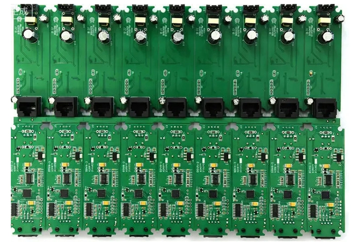
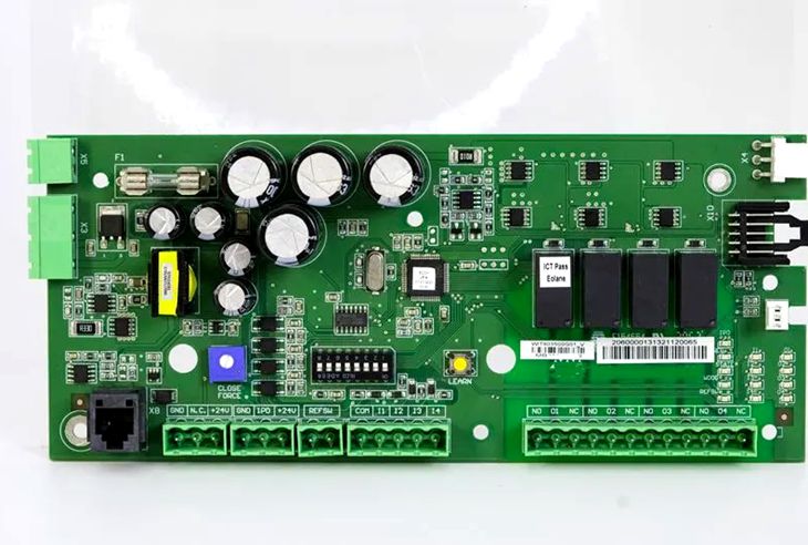
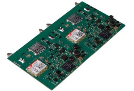
Modern IoT PCBAs frequently combine miniature passive components, fine-pitch integrated circuits, wireless modules, and mechanical connectors.
Surface Mount Technology (SMT) is typically used for automated placement of most electronic components.
The process begins with solder paste printing, followed by component placement and controlled reflow soldering.
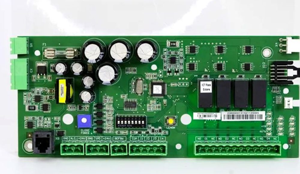
For boards containing through-hole connectors, terminal blocks, or other mechanically demanding parts, additional THT assembly may be required.
Manufacturers must coordinate these processes carefully.
For instance, heavy connectors may require special handling to maintain alignment, while temperature-sensitive parts may need a different assembly sequence.
Inspection methods should also match the component technology.
Automated Optical Inspection (AOI) is useful for identifying many visible placement and soldering defects. X-ray inspection can help evaluate hidden joints beneath suitable packages, including certain BGA devices.
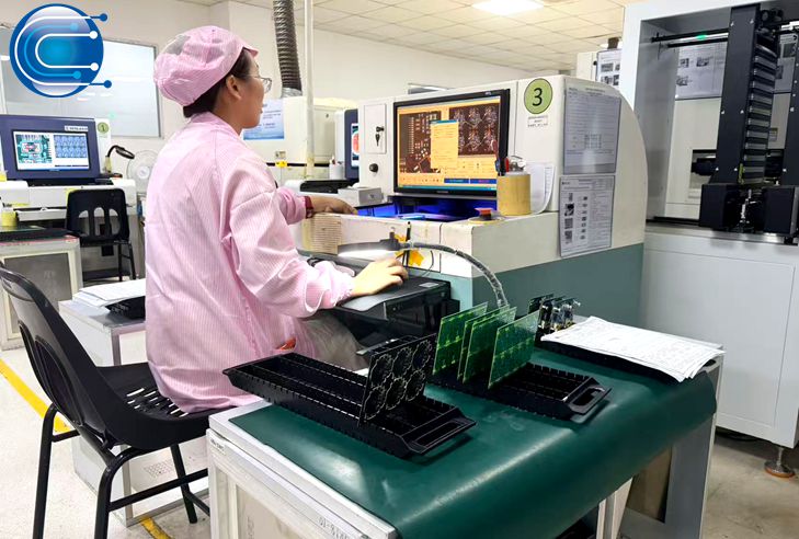
The objective is not to apply every available inspection method to every product. Instead, manufacturers should establish risk-based inspection coverage appropriate to the actual assembly.
4. Component Sourcing Can Determine Production Success
One of the biggest differences between prototype assembly and volume production is component availability.
Engineering teams may successfully assemble ten prototypes using readily available parts, only to discover that a critical microcontroller or wireless module has an extended procurement lead time.
For IoT devices, sourcing risks may affect processors, memory, RF components, sensors, power management ICs, and connectors.
A full-turnkey EMS partner can support the procurement process through BOM verification, supplier coordination, inventory planning, and approved alternative evaluation.
However, component substitutions require careful control.
An alternative component may share the same package while differing in electrical characteristics, firmware compatibility, temperature rating, or regulatory implications.
Therefore, substitutes should be reviewed and approved by the customer before implementation.
OEM buyers should also request information about component lifecycle status, sourcing channels, and traceability records.
These measures help protect production continuity without compromising the approved design.
5. Building a Reliable IoT PCBA Testing Strategy
Testing should be planned around the actual functions and failure risks of the device.
For example, an IoT gateway may require power rail verification, Ethernet interface checks, processor programming, and communication tests.
A wireless environmental sensor may instead require sensor calibration, current-consumption measurement, and wireless connectivity verification.
A typical manufacturing quality plan can combine several methods.
SPI checks solder paste printing before components are mounted.
AOI identifies visible assembly defects after soldering.
ICT or Flying Probe Testing verifies selected electrical characteristics where access and test coverage permit.
Functional Circuit Testing (FCT) checks defined operating functions using approved procedures.
For some products, additional thermal cycling, humidity exposure, or burn-in may be appropriate.
Nevertheless, the testing plan must distinguish between manufacturing verification and complete product qualification.
A PCBA passing functional testing does not automatically mean that the finished IoT device meets all environmental, wireless, or safety requirements.
6. Managing the Transition From NPI to Volume Production
New Product Introduction (NPI) connects engineering development with repeatable manufacturing.
During this stage, OEMs should validate not only circuit functionality but also production documentation, assembly yield, inspection coverage, and test procedures.
A useful NPI process may include initial engineering review, prototype assembly, first article inspection, issue reporting, and an approved production release.
As production quantities increase, additional attention should be given to process repeatability and materials planning.
Manufacturers should establish revision control so that the correct Gerber files, BOM versions, firmware releases, and assembly instructions are used for each order.
Production traceability can also help identify affected batches if a component or process issue is discovered later.
Furthermore, buyers should evaluate the total cost of manufacturing rather than the quoted assembly price alone.
Tooling, testing, component procurement, rework, packaging, and logistics can materially influence the final cost per accepted unit.
7. How Full-Turnkey EMS Supports IoT Manufacturing Growth
Coordinating separate PCB suppliers, component distributors, and assembly factories becomes more difficult as product volumes increase.
Full-turnkey EMS integrates these activities into a more unified manufacturing workflow.
This can reduce handoff errors, improve procurement visibility, and simplify communication during engineering changes.
For IoT OEMs managing multiple product variants, centralized BOM coordination and consistent inspection procedures may also support better production control.
However, successful outsourcing still requires clear responsibilities.
Customers should define approved components, revision requirements, testing criteria, and acceptance standards before production.
The EMS provider should then communicate manufacturing risks, sourcing constraints, and production status through an agreed process.
8. Ring PCB Manufacturing Support for IoT OEMs
Ring PCB provides PCB fabrication, component sourcing, SMT and THT assembly, engineering manufacturability review, inspection, and testing services for custom electronic assemblies.
Its full-turnkey EMS capabilities support OEM customers developing IoT gateways, industrial monitoring equipment, smart sensors, and other connected electronic products.
By coordinating PCB production, material procurement, and assembly under one manufacturing workflow, Ring PCB helps customers simplify supplier management and prepare for repeat production.
Customers can submit Gerber files, BOMs, placement data, and project-specific test requirements for review.
For IoT PCBA manufacturing inquiries: rfq@ringpcb.com
Conclusion
Scaling IoT hardware requires more than increasing assembly quantities.
Successful production depends on manufacturable PCB designs, controlled SMT processes, reliable component sourcing, appropriate testing, and disciplined engineering revision management.
OEMs that address these requirements early can reduce avoidable production disruptions and establish a stronger foundation for long-term connected-device manufacturing.