At Ring PCB,as a professional manufacturer and customizer of PCB and PCBA for over 17 years,we operate 5,000+㎡ modern self-owned factories in Shenzhen and Zhuhai, China, with a 500-strong team. All our PCB and PCBA products adhere to international industry standards.
Need a prototype? We deliver in 3 days.
Mass production? Ready in 7 days. Our solutions have reached over 50 countries and regions, backed by full-turnkey PCBA services tailored to your needs.
In the past 17 years, Ring PCB has served more than 20,000 domestic and overseas customers to customize various types of PCB boards and PCB assembly services.
Why Choose Ring PCB?
Core Competencies & Advantages of Ring PCB Technolog
1. Direct Factory Pricing & Transparent Manufacturing
◦ Owned Shenzhen factory ensures source-level cost control and eliminates middleman markups.
◦ Invitation for factory visits to witness advanced equipment (e.g., automated SMT lines) and rigorous production processes firsthand.
2. One-Stop PCB & PCBA Expertise for End-to-End Solutions
◦ Comprehensive services from 2-48 layer PCB fabrication to components sourcing, SMT assembly, and full turnkey projects, eliminating the need for multiple vendors.
◦ 17+ years of industry experience (since 2008) with 500+ skilled employees, delivering 5,000+ electronic projects for 3,000+ global clients.
3. Stringent Quality Control with Advanced Inspections
◦ Multi-stage quality assurance: SPI 3D, AOI, LCR testing, and X-Ray for BGA components ensure zero-defect products.
◦ Certified compliance: IPC standards, RoHS, UL, ISO 9001/14001/13485, IATF16949—meeting medical, automotive, and industrial safety requirements.
4. Industry-Leading Capabilities & Customization
Specialized in high-frequency, heavy copper, and complex PCBs for demanding sectors: communication base stations, medical devices, EV charging stations, robotics, etc.
Tailored solutions for unique projects—from prototype to mass production, with rapid turnaround supported by in-house Shenzhen factory.
5. Reliable Partner for Diverse Applications
Wide industry coverage: Security, industrial control, drones, servers, and more—proven track record in critical sectors requiring high reliability.
Incoming material inspection, real-time process monitoring, and final QC guarantee on-time delivery with consistent performance.
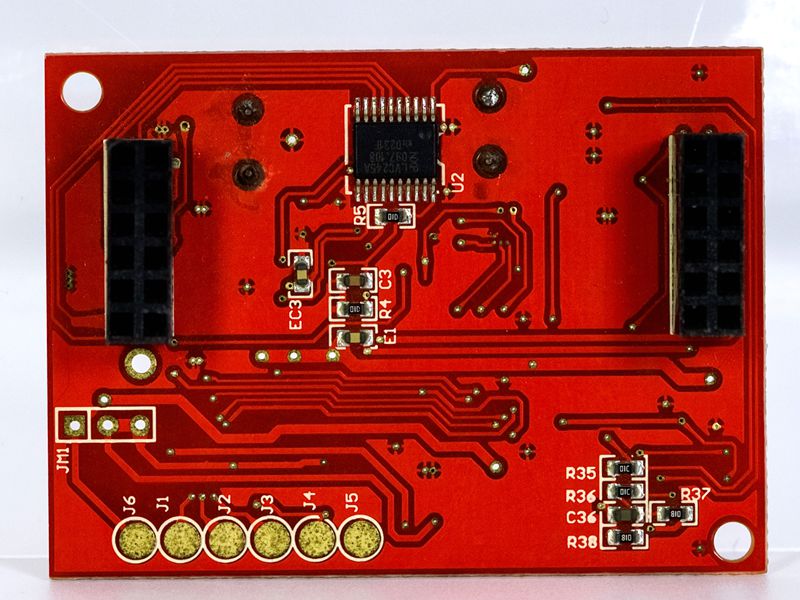
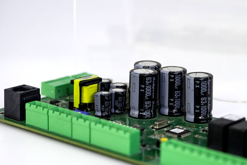
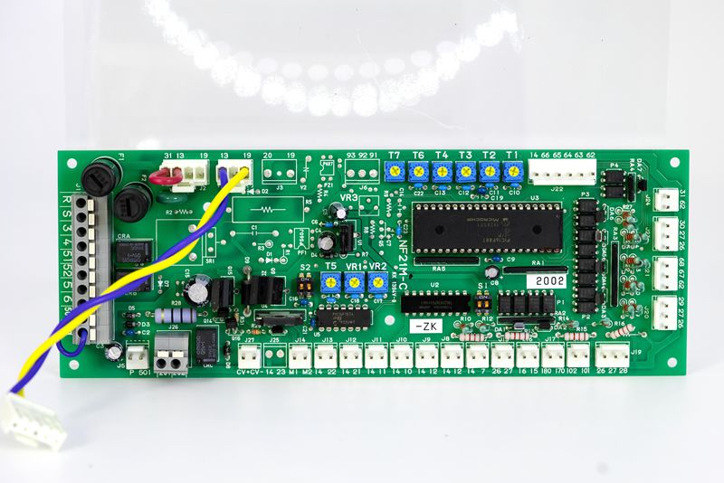
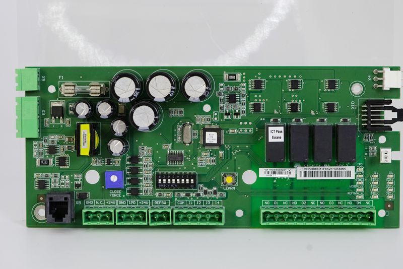
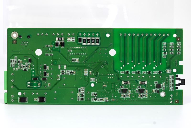
Customizable IoT Device PCB Assembly - Tailored Solutions for Connected Systems
1.Product Features of IoT PCB Assembly
- High-Frequency Signal IntegritySupports advanced wireless protocols (5G, Wi-Fi 6E, Bluetooth 5.3) with precise impedance control and low dielectric loss materials like Rogers RO4003C.
- Ultra-Low Power ConsumptionOptimized for battery-driven devices (e.g., 8μA standby current) with power management ICs (PMICs) and sleep-mode circuit design.
- Miniaturization & High DensityIntegrates 01005/0201 passive components, system-in-package (SiP) technology, and HDI (High-Density Interconnect) for compact layouts.
- Flexible & Rigid-Flex DesignCombines rigid FR-4 and flexible polyimide layers for curved devices (e.g., smartwatches).
- Thermal ManagementCopper cladding and heat spreaders reduce hotspot temperatures by 15-30% in high-power modules.
- Environmental ResilienceUses 3D coating and RoHS-compliant materials for salt fog, UV, and extreme temperature resistance.
2.Advantages of IoT PCB Assembly
- Rapid Time-to-MarketThree-month iteration cycles via flexible manufacturing lines (e.g., 10-minute changeover for small batches).
- Cost-Effective ScalabilityEliminates high-volume penalties with modular production (e.g., 100-100,000 units at similar costs).
- Signal ReliabilityHybrid stack-up and controlled impedance ensure <5% signal loss in 5G/mmWave applications.
- Green ManufacturingENIG/OSP finishes and halogen-free materials meet EU environmental standards.
- Multi-Domain CompatibilitySupports simultaneous operation of sensors, RF modules, and microcontrollers with EMI shielding.
3.Technical Challenges in IoT PCB Assembly
- Precision Soldering01005 components require SPI (3D solder paste inspection) + AOI + X-ray for <5% voiding in BGA joints.
- High-Frequency LayoutMillimeter-wave routing demands <10μm linewidths and hybrid laminates (e.g., Megtron 6 + Rogers).
- Thermal Expansion ControlCTE mismatch between copper (17ppm/°C) and FR-4 (13ppm/°C) risks delamination in multi-layer boards.
- EMC ComplianceRequires ground planes and differential pairs to mitigate interference between Wi-Fi and sensor signals.
- Material SelectionBalancing dielectric constant (Dk) and cost: Rogers RO4003C (Dk=3.38) vs. standard FR-4 (Dk=4.4).
Technical Parameters of IoT PCBA
| Parameter | Specifications |
| Layer Count | 1-40 layers (standard: 2-16 layers). |
| Copper Thickness | 0.5-14 oz (17.5-490μm); 1-3 oz typical for IoT. |
| Minimum Line/Space | 2.5/2.5 mil (0.0635mm) for HDI. |
| Microvia Diameter | 0.08-0.15mm (stacked/buried vias). |
| Material Options | FR-4 (Tg 130-170°C), Rogers RO4003C (Dk=3.38), and aluminum cores. |
| Inspection Methods | AOI (automated optical inspection), X-ray (BGA void analysis), and ICT (in-circuit test). |
| Surface Finishes | ENIG, OSP, HASL (lead-free), and gold plating. |
| Thermal Resistance | <10°C/W with copper cladding (0.1mm thickness). |
| RoHS Compliance | Halogen-free, lead-free, and REACH-certified materials. |
| Operating Temperature | -40°C to +125°C (industrial grade). |
From startups to OEMs — we help your product succeed.
Email: rfq@ringpcb.com
https://www.ringpcb.com/
Are you looking for a seamless experience in PCB manufacturing, assembly, and component procurement? Look no further than Ring PCB. Our comprehensive services cover every aspect of your project!


