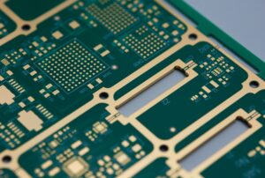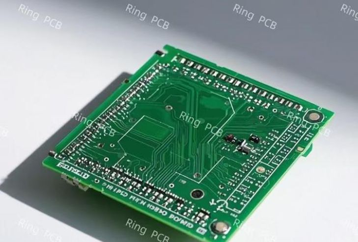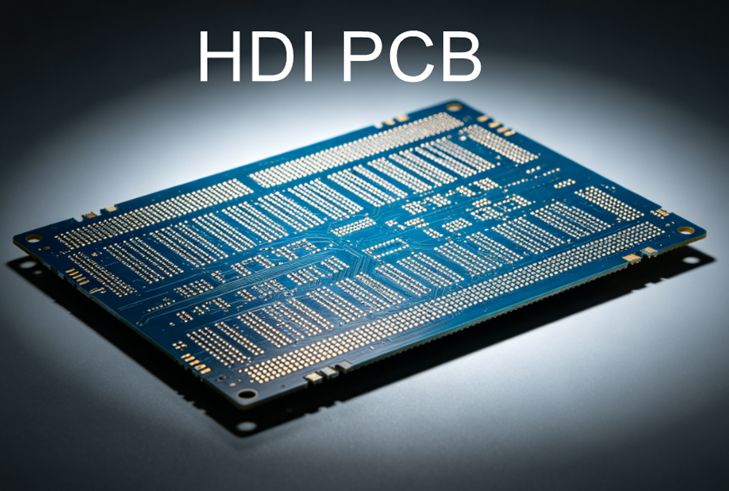
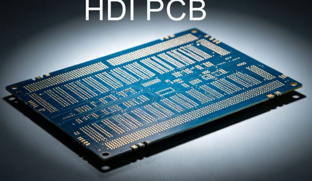
As electronic products become smaller and more powerful, printed circuit boards must accommodate more components, finer routing, and increasingly complex interconnections within limited space. High-Density Interconnect (HDI) technology addresses these challenges by using finer lines and spaces, microvias, and advanced layer structures to increase routing density.
For OEMs in telecommunications, automotive electronics, medical devices, and computing, choosing an HDI PCB is not simply a matter of fitting more circuits onto a smaller board. The manufacturing process, microvia reliability, material selection, and production yield all influence the final product’s performance and cost.
The market outlook also reflects the growing importance of advanced PCB technologies. Prismark’s 2026 industry forecast, as reported in a recent market analysis, projects HDI PCB production value to increase from approximately USD 16.2 billion in 2025 to USD 19.92 billion in 2026, representing forecast growth of about 23%. This is a market-value forecast, not a measurement of physical board shipments. Nevertheless, it indicates that HDI is among the faster-growing PCB technology segments. [Source: Prismark Q1 2026 forecast, reproduced in DETUS’s 2026 PCB industry report.]
1. What Makes HDI PCB Different from Conventional Multilayer PCB?
HDI PCBs are designed to achieve higher interconnection density than conventional PCB structures. They typically use finer conductor geometries, smaller vias, and build-up layers to connect densely arranged components.
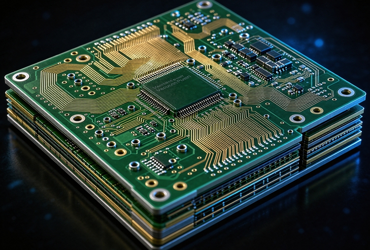
A conventional multilayer PCB often relies mainly on mechanically drilled through-holes that pass through the full board thickness. HDI structures can incorporate laser-drilled microvias, blind vias, and buried vias to connect selected layers without using a through-hole for every interconnection.
This provides more routing flexibility and can help reduce board size. It is particularly useful for products that use fine-pitch components, compact modules, or high-density component placement.
However, HDI is not automatically the best option for every product. If a conventional multilayer structure can meet the electrical and mechanical requirements at a lower cost, it may remain the more practical solution. The decision should be based on routing density, component pitch, available board area, electrical performance, and total manufacturing cost.
2. Understand the Role of Microvias and Build-Up Technology
Microvias are a defining feature of many HDI constructions. They are typically created using laser drilling and connect adjacent or selected layers within the PCB stackup.
Depending on the design, HDI boards may use:
- Blind vias connecting an outer layer to an inner layer
- Buried vias connecting internal layers
- Stacked microvias connecting multiple build-up layers vertically
- Staggered microvias connecting layers with offset positions
- Sequential lamination to build up the required layer structure
These structures allow designers to route signals through dense areas while preserving space for components and other electrical connections.
Nevertheless, microvia selection has manufacturing implications. Stacked structures can reduce routing space, but they also introduce demanding requirements for laser drilling, copper plating, layer registration, and interface integrity. Staggered structures may offer different manufacturing and reliability trade-offs.
Therefore, buyers should not evaluate microvia technology only by the number of connections it enables. The chosen structure must also be compatible with the manufacturer’s process capability and the product’s reliability requirements.
3. Microvia Reliability: Look Beyond Hole Dimensions
Microvia reliability is one of the most important considerations in advanced HDI manufacturing.
Historically, engineers have paid close attention to parameters such as via diameter, aspect ratio, plating thickness, and annular ring dimensions. These remain important. However, recent technical research highlights that reliability can also depend heavily on the quality of the buried copper interfaces within a microvia.
A 2026 review published in Advanced Materials & Sustainable Engineering discusses how the interface between electroless copper and the target copper layer can influence microvia degradation. The research points to factors such as surface preparation, seed-layer continuity, laser drilling, and electroplating as contributors to interface quality.
This has a practical implication for OEMs: a microvia that meets visible dimensional requirements is not necessarily free from latent reliability risks.
When evaluating an HDI manufacturer, ask how it controls the complete microvia process, including:
- Laser drilling accuracy and consistency
- Desmear and surface conditioning
- Electroless copper deposition
- Electroplating and copper filling
- Layer-to-layer registration
- Process qualification and reliability testing
For products exposed to thermal cycling or demanding operating environments, the agreed qualification plan should reflect the actual application. Inspection and testing methods should be confirmed with the supplier rather than assumed to be included in every standard production order.
4. Material Selection for High-Speed and High-Density Applications
HDI designs often combine routing density with demanding electrical performance. Material selection should therefore consider more than the nominal laminate type.
FR-4 remains widely used in many HDI applications. However, high-speed or high-frequency circuits may require materials with more tightly controlled dielectric properties and lower signal loss.
Important material parameters include dielectric constant (Dk), dissipation factor (Df), glass transition temperature (Tg), coefficient of thermal expansion (CTE), and thermal performance. The appropriate balance depends on signal frequency, layer construction, operating temperature, and reliability expectations.
AI infrastructure and high-performance computing are also influencing the broader PCB material supply chain. The Printed Circuit Engineering Association reported in June 2026 that strong demand for AI servers was supporting growth in high-layer-count PCB materials and advanced copper-clad laminates. Its report highlighted the development of low-Dk glass fabric, quartz fabric, and PTFE-based materials for high-speed applications.
For buyers, material availability should be considered early. A technically suitable laminate may have different lead-time or sourcing conditions from standard FR-4. Any alternative material should be reviewed against the project’s electrical and mechanical specifications before approval.
5. How HDI Technology Supports AI, Telecom, and Compact Electronics
HDI technology is used in applications where component density and routing efficiency are critical.
Telecommunications equipment: High-density routing can support compact networking modules, communication devices, and complex signal paths.
Automotive electronics: Advanced driver assistance systems, infotainment, control modules, and sensing applications may require compact boards with dense component placement.
Medical electronics: Portable and compact medical devices can benefit from smaller circuit assemblies, provided that the PCB meets the applicable reliability and product requirements.
Computing and AI infrastructure: High-performance systems place increasing demands on interconnection density, signal integrity, and power distribution. Not every AI server board is an HDI board, but advanced HDI structures are relevant in selected modules and compact high-density assemblies.
These applications do not share identical requirements. A telecommunications module may prioritize signal integrity, while an automotive control unit may place greater emphasis on thermal cycling and long-term reliability. The manufacturing specification should reflect the actual use case.
6. Control HDI Cost Through Stackup and Process Planning
HDI PCBs can cost more than conventional multilayer boards because they may require sequential lamination, laser drilling, additional plating steps, finer imaging, and more demanding inspection.
The cost impact depends on the number of build-up layers, microvia structure, material system, board dimensions, panel utilization, and production volume.
A practical way to control cost is to avoid unnecessary complexity. For example, not every signal connection needs a microvia, and not every design requires stacked microvias. Where the electrical and mechanical requirements permit, alternative routing or via arrangements may reduce process steps.
OEMs should also consider the cost of yield loss and rework. A lower initial quotation may not represent better value if the construction is close to the manufacturer’s process limits.
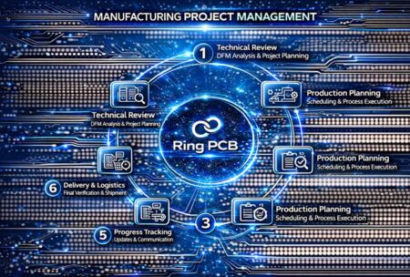
Before production, clarify the required layer structure, via types, material grades, minimum feature sizes, tolerances, and inspection expectations. A clear technical package helps the manufacturer assess manufacturability and identify questions before the order is released.
7. What to Ask an HDI PCB Manufacturer Before Ordering
A focused supplier review can help procurement and engineering teams reduce technical and commercial risk.
- What HDI layer structures and sequential lamination processes can the supplier support?
- What microvia diameters, depths, and structures are available for the proposed construction?
- How are laser drilling, desmear, copper deposition, and plating controlled?
- What material grades are available, and how are substitutions handled?
- What inspection and reliability tests are included in the quotation?
- Can the supplier support prototype evaluation and repeat production?
- How are engineering questions, process changes, and nonconforming products communicated?
The supplier’s response should be specific to the proposed board construction. General statements about advanced equipment are not a substitute for confirming the actual manufacturing window.
Working with Ring PCB
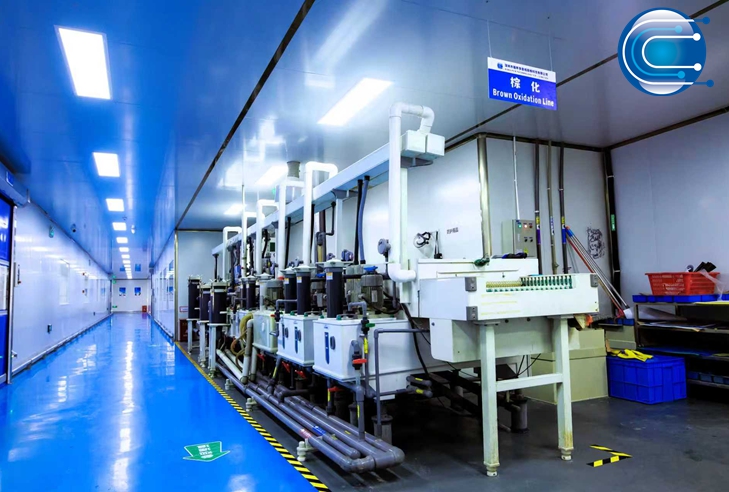
For projects involving rigid multilayer PCB fabrication and PCBA, Ring PCB provides PCB manufacturing, component sourcing, SMT assembly, through-hole assembly, and production quality inspection. Established in 2008, the company operates a self-owned manufacturing facility covering more than 10,000 square meters and supports rigid PCB manufacturing of up to 62 layers.
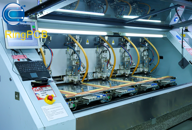
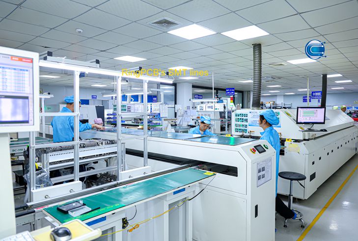
Its five automated SMT production lines support PCB assembly requirements, while first article inspection equipment helps verify production setup. PCB prototypes may be available in as little as 72 hours, depending on board specifications, material availability, and project requirements.
Customers can submit Gerber files, BOM information, and technical specifications for manufacturing communication and feasibility review. For HDI projects, the exact microvia structure, material system, and process requirements should be confirmed against the specific manufacturing scope before order placement.
For PCB fabrication and PCBA inquiries, contact:rfq@ringpcb.com
References and Sources
- DETUS — PCB Manufacturing Industry Report 2026, reporting Prismark Q1 2026 market forecasts
- Printed Circuit Engineering Association — Market Watch, June 2026
- Advanced Materials & Sustainable Engineering — Interface-Controlled Reliability of HDI Microvias: A Critical Review and Perspective, May 2026
- Ring PCB — Company manufacturing information, www.ringpcb.com