
For two decades, most sourcing conversations about printed circuit boards started with price per square meter and a promised delivery date. That framing no longer holds. Global PCB output is forecast to reach roughly USD 95.7 billion in 2026, up about 12.5% year over year, yet growth inside that number is sharply uneven. HDI is expanding at roughly 14.5%, while boards above 18 layers climbed an estimated 72.8% in 2025 and a further 62.4% in 2026. Analysts tracking the mix expect the 30-plus-layer slice to move from about 12% of multilayer revenue in 2025 to 18% in 2026, and to approach the mid-forties by 2027.
The headline is not simply that the market is bigger. It is that the average board is harder to build, and the list of suppliers able to build it is shorter than the order book assumes.
Why Layer Counts Keep Climbing
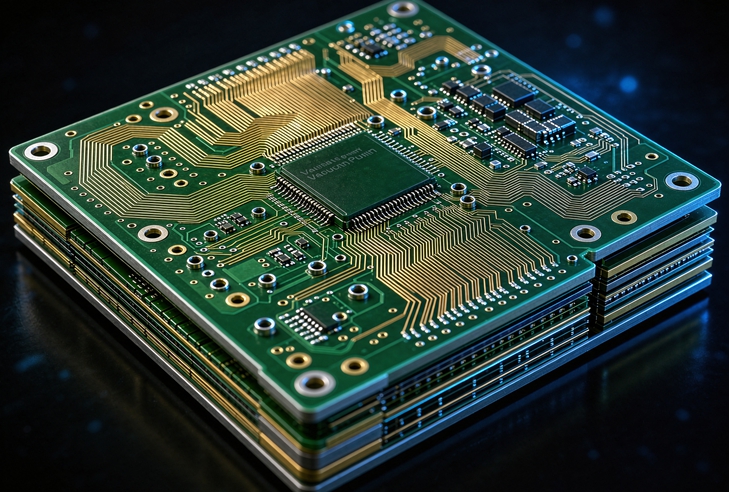
AI accelerators pulled the whole stack upward. A GPU server board that once used 10 to 12 layers now routinely runs 20-plus, and premium models reach 34 to 64 layers. Nvidia’s Rubin Ultra NVL576 backplane is reported at 78 layers on M9-class laminate, replacing internal copper cabling with a single orthogonal board. Server PCB shipment area is projected to rise from roughly 0.9 million square meters in 2025 to 4.5 million by 2028, while blended ASP per square meter climbs from about USD 5,833 to USD 18,549. Value has migrated from area to complexity.
Signals follow. At 112 Gbps and above, insertion loss budgets tighten to under 30 dB across a 30-inch trace, which forces designers to shorten via stubs below 5 mil, hold controlled impedance to a few percent, and move to low-loss laminates. None of that is achievable on a stack that was qualified for a 8-layer consumer board.
Where Conventional Fabrication Breaks Down
Higher layer counts attack the process rather than the drawing. Four failure modes dominate.
Registration drift. Each lamination cycle stacks tolerance on tolerance. On a 6-layer board a 2 mil misregistration is absorbed by design margin; on a 40-layer board the same error can short an inner layer or open a signal path.
Resin flow and thickness control. Sequential lamination changes the dielectric thickness between layers, which shifts impedance on every high-speed pair at once.
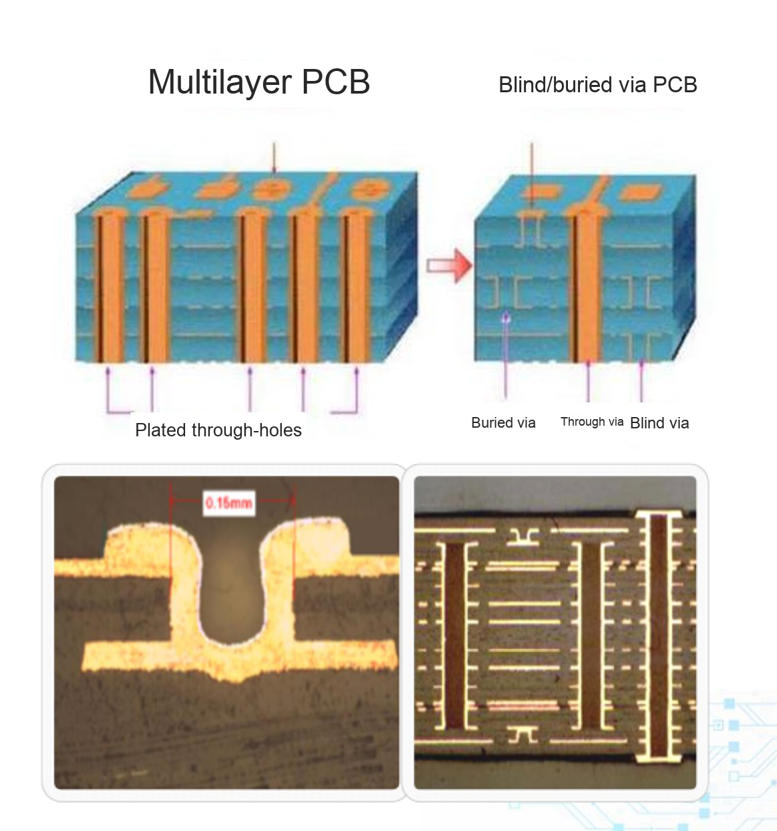
Drill behavior at depth. Mechanical aspect ratios of 20:1 and beyond bend bits, smear sidewalls and produce plating variation inside the barrel. Laser microvias behave differently again: diameter, taper and target pad all need process control, not operator control.
Via stubs. A long stub turns into a resonant network at multi-gigabit rates. Backdrilling has to be a specified, measured process with a stub tolerance in mil, not a checkbox on a capability sheet.
Six Questions Buyers Should Actually Ask
Instead of asking whether a fabricator can build 30 layers, ask for the answer in two columns.
- Sample versus volume. What is your maximum layer count at prototype, and what is it at volume? A single number is a marketing number.
- Aspect ratio at production, not just at sample.
- Microvia diameter and stack type — 2+N+2, or any-layer HDI?
- Via-in-pad treatment — resin or copper paste fill, with plating over fill (POFV)?
- Backdrill stub control, expressed in mils.
- Mixed lamination — can FR-4, high-Tg and PTFE-class materials run in one stack without yield collapse?
Conversationally, procurement teams increasingly score fabricators on yield stability, microvia reliability and laminate access rather than on unit price alone.
How RingPCB Answers Those Questions
We publish both columns, because we build to both.
Sample builds run to 70 layers, 0.2–10 mm board thickness, 2.0/2.0 mil trace and space on half-ounce copper, 0.125 mm mechanical drills, 30:1 mechanical aspect ratio, laser vias from 0.075 mm to 0.5 mm, and ELIC HDI.
Volume production is set at 30 layers, 0.3–6.0 mm, 2.5/2.5 mil, 0.15 mm drills, 15:1 aspect ratio and 2+N+2 HDI, with impedance held to ±10% and backdrill stubs of 8–16 mil, tightening to ±5% and 0–8 mil in prototype.
Copper capacity reaches 20 oz on samples and 12 oz in series, which covers high-current power sections on the same panel as fine-line digital routing. POFV, drilled blind and buried vias, depth-controlled milling, edge plating and hybrid dielectric stacks are process options rather than exceptions. Finish options include ENIG, immersion tin, immersion silver, plated silver, OSP, OSP+ENIG, HASL (lead and lead-free), gold finger plus ENIG and hard gold plating. Laminate supply spans SYE, ITEQ, TUC, Panasonic, Rogers, Taconic, Isola, Ventec, KB and HZ.
The Sourcing Consequence
Supplier qualification now has to happen twice — at prototype and at ramp — using the same parameters. A supplier that wins the sample and loses the volume build costs a program a full quarter, sometimes two. That is why the two-column question matters more than any single capability claim.
If your next board sits at 20 layers or above, uses microvias below 0.1 mm, or needs a stub under 8 mil, treat process capability as a gating item and confirm it before you release Gerber files.
RingPCB manufactures from customer-supplied Gerber files and BOMs, supports 72-hour rapid prototyping and flexible small-batch orders, and runs PCBA assembly with component sourcing alongside fabrication. Our engineering team reviews stack-up, drill schedule and finish selection for producibility before quoting, so the gap between prototype and volume is visible early rather than discovered late.
Send your Gerber files and BOM to rfq@ringpcb.com for a technical review.