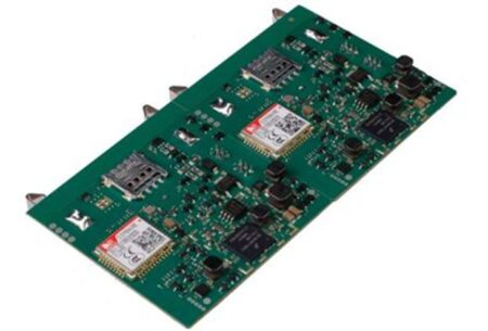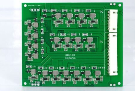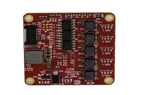

Against the backdrop of AI computing, electric vehicles and industrial IoT expansion, multilayer PCB has evolved from optional upgrade to core hardware foundation for modern electronics. Global PCB market revenue is projected to hit 85‑90 billion USD in 2026, with multilayer products contributing the largest share of growth, driven by server, automotive and medical electronics demand. Many B‑end hardware engineers and procurement teams face real‑world pain points including material shortage, extended lead‑time and unstable batch consistency when sourcing multilayer PCBs. This article breaks down core industry shifts and practical insights for project decision‑making.
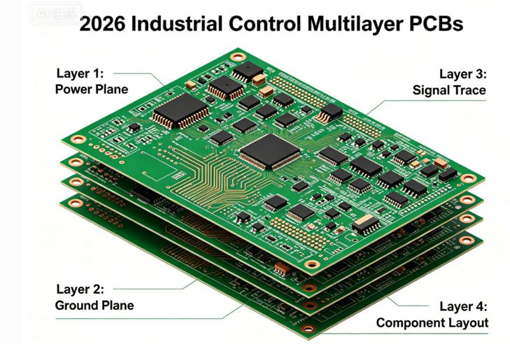
Rising Demand for Higher‑Layer‑Count & Low‑Loss Materials
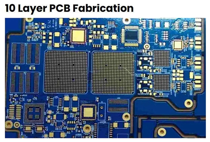
First of all, layer‑count requirements keep climbing. Traditional 4‑6‑layer boards still dominate general industrial projects, while AI server and high‑speed communication hardware widely adopt 16‑22‑layer stack‑ups, and some advanced computing boards reach 30+ layers. Meanwhile, low‑loss dielectric materials are gaining wider adoption. High‑frequency signals require stable DK/Df parameters to restrain signal attenuation, which brings higher requirements for raw material supply chain.
Nevertheless, material supply tightness remains a major industry bottleneck in 2026. High‑Tg prepreg, low‑loss resin and specialized copper foil face periodic supply pressure, which directly pushes up cost and prolongs production cycles for complex multilayer orders. Many small‑scale PCB manufacturers cannot secure stable material inventory, resulting in unexpected project delays for their customers.
Core Pain Points Faced by B‑End Multilayer PCB Buyers
In the procurement practice, three challenges repeatedly trouble hardware teams. To begin with, lamination‑related hidden defects are hard to detect. Interlayer mis‑registration, inner‑layer delamination and micro‑voids inside prepreg often cannot be caught by basic flying‑probe testing, and only appear after long‑term temperature cycling on end‑products. Secondly, lead‑time volatility creates scheduling risk. Standard multilayer PCB lead‑time averages 4‑6 weeks, while high‑layer low‑loss boards may extend to 14‑20 weeks during peak demand seasons. Thirdly, cost transparency is poor. Buyers frequently receive greatly divergent quotations without clear explanations for material, yield loss and testing expenses.
Consequently, simply picking the lowest‑price offer often leads to expensive rework or product recall at later development stages.
How Qualified PCB Manufacturers Mitigate Multilayer‑Related Risks
Reliable multilayer PCB manufacturers do not only focus on finished‑board electrical testing. Instead, they implement full‑process quality control starting from Gerber DFM review. Professional engineering teams verify stack‑up symmetry, layer‑alignment tolerance and material compatibility before production starts, to avoid manufacturability risks embedded inside original design files. During fabrication, inner‑layer AOI, lamination parameter monitoring and cross‑section sampling inspection serve as critical gates to catch hidden inter‑layer defects.
For over 18 years, Ring PCB has accumulated rich experience in multilayer PCB fabrication from prototype to mass production. We maintain long‑term partnerships with mainstream substrate suppliers and keep safety stock for high‑Tg, low‑loss and heavy‑copper materials, easing the impact of global material fluctuation on client projects. Our in‑house engineering team provides free DFM stack‑up evaluation for multilayer projects, helping customers balance performance, manufacturability and total budget. We support 4‑32 layer rigid multilayer PCBs, covering industrial, medical, EV charger and high‑speed computing scenarios.
If you have ongoing multilayer PCB projects and want to get professional evaluation or quotation, feel free to send your Gerber files to rfq@ringpcb.com.