
Ring PCB – Fast PCB Prototype & Full Turnkey PCBA Solution
Product Overview
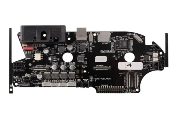
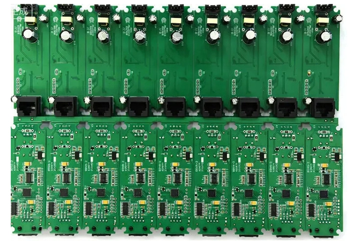
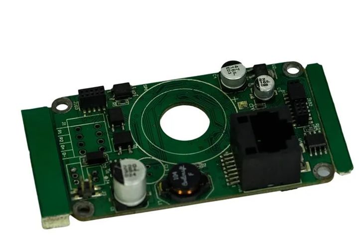
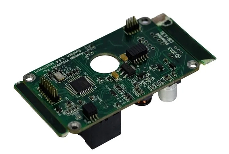
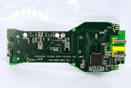
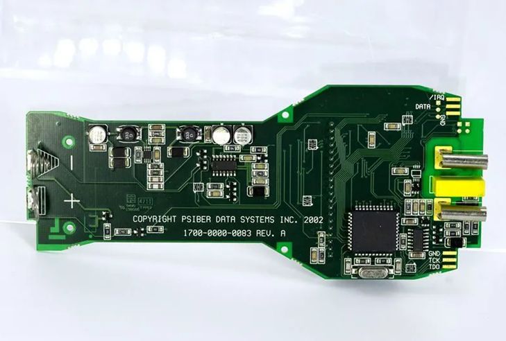
This custom irregular-shaped PCBA serves as a professional data communication interface board, developed for signal transmission and data acquisition systems. Equipped with a main microcontroller chip, passive components, power regulation circuits and dedicated signal test pins, the assembly supports stable data communication and signal conversion. Classified under PCBA For Communication, it is widely applied in data test equipment, industrial signal converters and portable data interface hardware.

Ring PCB provides customized and OEM PCBA manufacturing service for communication interface boards. We support full development customization according to customers’ Gerber files, BOM and technical specifications, covering prototype verification and mass production.
Key Features
- Custom irregular PCB outline design to fit compact enclosure space of portable data devices.
- Integrated MCU control circuit with complete power supply regulation to guarantee stable continuous operation.
- Reserved dedicated signal test pins (DATA, TCK, TDO, GND and other interfaces) for convenient debugging and signal monitoring.
- Optimized signal routing layout to reduce electromagnetic interference and improve data transmission stability.
- Mature SMT assembly process, supporting dense small passive components and IC mounting for compact circuit design.
Product Specifications
| Item | Parameter |
|---|---|
| Product Name | Communication Interface Data Acquisition PCBA |
| Category | PCBA For Communication |
| PCB Shape | Custom Irregular Outline |
| PCB Layers | 2L ~ 8L Multilayer PCB (Customizable) |
| Base Material | FR-4 |
| Surface Finish | ENIG, OSP, HASL (Optional) |
| Assembly Process | Precision SMT + Selective Hand Soldering |
| Core Function | Signal conversion, data transmission, data acquisition |
| Standard Compliance | RoHS, REACH, IPC-A-610 Class 2 |
| Application | Data test equipment, communication signal interface modules, portable data debugging tools |
The above technical parameters are for your reference only. If you wish to customize other types of communication equipment PCBA, please provide your drawings or technical parameters to our staff. For details, please consult our online customer service. Thank you for your cooperation.
Ring PCB Service & Advantages
✅ Customization & OEM Service Available We fully support OEM and personalized custom development. Adjust PCB outline, circuit layout, interface configuration and component matching according to your unique project requirements.
✅ Full Turnkey EMS One-Stop Solution Services include bare PCB fabrication, authorized component sourcing, SMT assembly, BGA rework, ICT testing and functional aging test. You only need to provide design documents.
✅ High Precision Manufacturing Capacity Experienced in HDI multilayer boards and large BGA component mounting, meeting the strict requirements of notebook mainboard assembly.
✅ Complete Quality Control System All products pass AOI, X-Ray inspection for BGA chips and electrical testing before delivery. ISO9001, UL certified factory guarantees consistent batch quality.
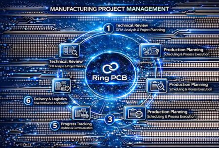
✅ Free DFM Engineering Support Our technical team provides free DFM analysis at the early design phase, discovering potential manufacturing risks and optimizing your design to save costs and shorten lead time.
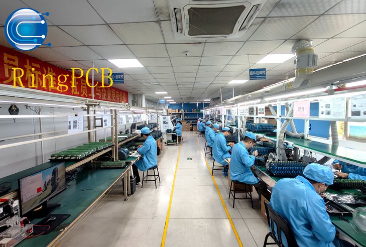
RingPCB Manufacturing Strength & Full Turnkey Services
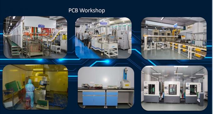
Our complete quality inspection process includes X-ray internal solder void detection, RF signal performance testing, thermal cycling aging, damp heat corrosion test and full-load 72-hour burn-in, with complete traceable test reports provided for every batch of communication PCBA. We adopt dual-source supply for core RF chips, MCUs and connectors to avoid production delays caused by component out-of-stock, stably supporting sample orders and mass production ranging from hundreds to tens of thousands of units.
Authorized Global Industry Certifications
Contact Us
📧 Email: rfq@ringpcb.com