Product Description
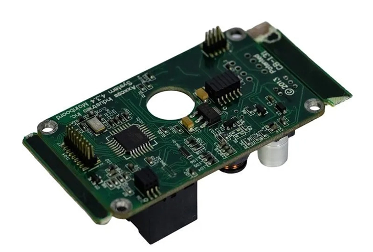
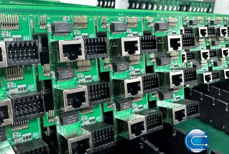
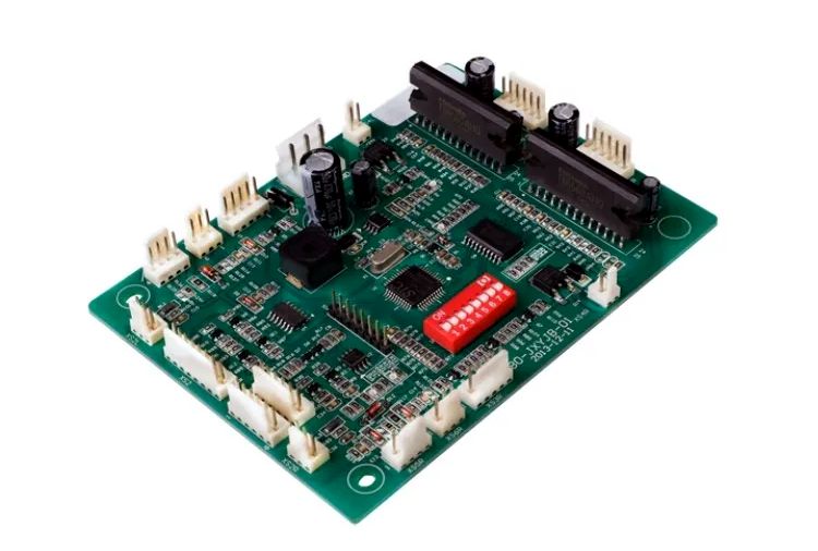
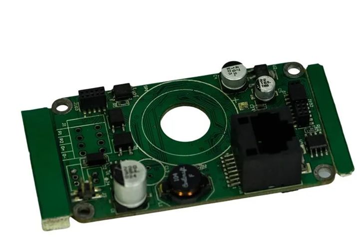
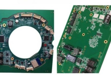
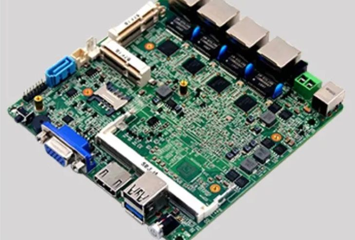
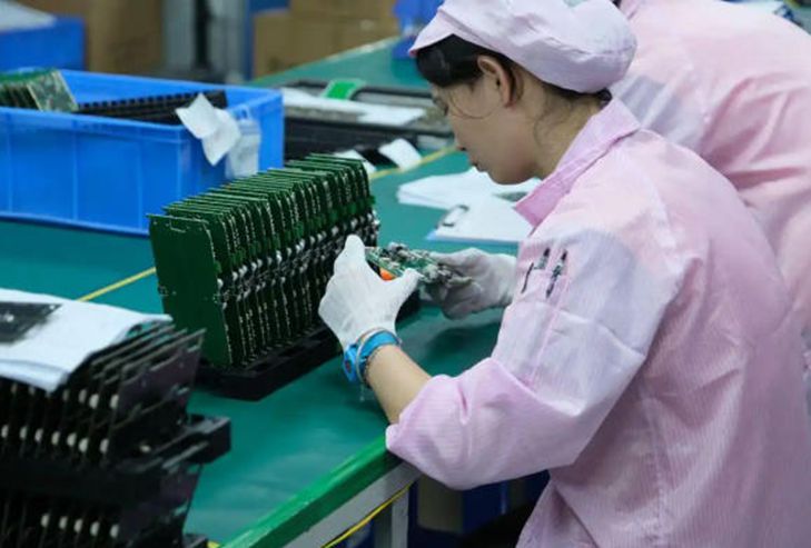
Ring PCB, we offer one-stop OEM & ODM assembly for all types of communication mainboards, with professional DFM optimization and complete reliability testing to guarantee stable performance for mass-produced smart robotics equipment.
1.What are Communication PCBAs?
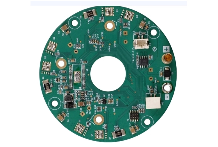
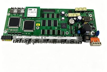
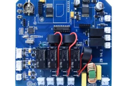
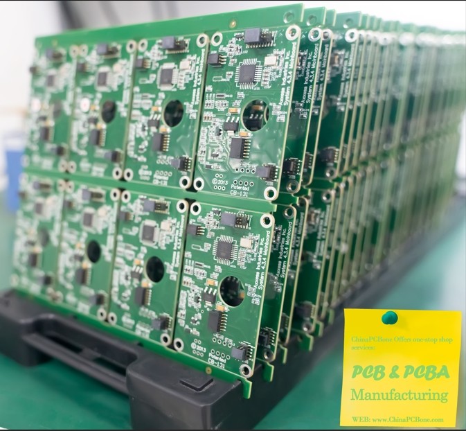
Communication PCBA (Printed Circuit Board Assembly) refers to a printed circuit board that has been populated with electronic components and is specifically designed for communication – related applications. It serves as the core component in various communication devices, such as routers, wireless access points, mobile phones, and base stations. It integrates multiple electronic components like microcontrollers, radio – frequency chips, and connectors through a complex network of conductive traces on the printed circuit board to enable functions like signal processing, transmission, and reception.
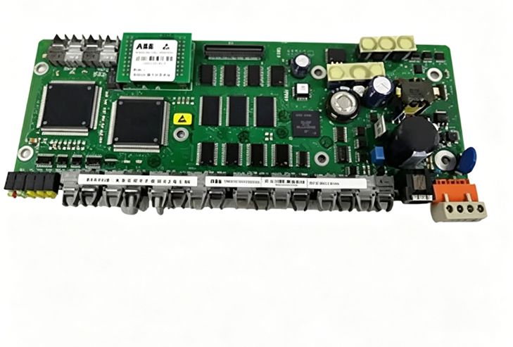
2.The Characteristics of Communication PCBAs?
-
High – Frequency Performance: It is engineered to handle high – frequency signals effectively. This is crucial for communication devices operating in radio – frequency bands, ensuring minimal signal loss and interference during transmission and reception.
-
Miniaturization: With the trend towards smaller and more portable communication devices, Communication PCBA often features a high – density component layout. Components are packed closely together, and advanced manufacturing techniques are used to reduce the overall size of the board while maintaining functionality.
- Reliability: Since communication devices are expected to operate continuously and stably, PCBA for communication applications is designed with high – quality materials and strict manufacturing standards. It has to withstand various environmental conditions and long – term use without significant degradation in performance.
- Integration: It integrates multiple functions such as data processing, modulation, demodulation, and communication protocol implementation. This integration simplifies the design and manufacturing process of communication devices and also improves their overall performance.
- Customizability: Different communication devices have different requirements. Communication PCBA can be customized according to specific application needs, such as adjusting the communication frequency band, data transfer rate, and power consumption.
In the past 18 years, RingPCB has served more than 20,000 domestic and overseas customers to design and customize various types of PCB boards and PCB assembly manufacturing services.
3.The Importance of Communication PCBA
Communication PCBAs are used in a wide array of devices, including:
Base Stations for mobile networks.
Routers and Modems for internet connectivity.
Satellite Communication Systems for global coverage.
Optical Networking Equipment for high-speed data transfer.
IoT Devices that connect smart technologies.
Common Technical Parameters
| Parameter | Specification |
|---|---|
| PCB Layers | 6–16 Layers |
| Board Thickness | 0.8 – 2.4 mm |
| Line Width / Spacing | 0.1 – 0.3 mm |
| Surface Finish | ENIG, HASL, OSP |
| Operating Temperature | -40°C to +85°C |
| Signal Frequency | kHz – GHz |
| Assembly Accuracy | ±0.05 – 0.1 mm |
| Insulation Resistance | ≥1000 MΩ |
All above parameters are for reference only. We provide exclusive customized services. Please submit your Gerber files and application requirements via email to rfq@ringpcb.com to consult our professional technical team for detailed specifications and technical demands.
Why Choose Ring PCB?
18 Years of Manufacturing Excellence
Self-owned factory with full process control.
One-Stop Full Turnkey Service
PCB fabrication + component sourcing + SMT assembly + functional testing.
Advanced Production Equipment
LDI exposure, vacuum lamination, AOI, X-ray inspection, flying probe testing.
Reliable Soldering Technology
8-stage lead-free reflow soldering and wave soldering ensure assembly stability and RoHS compliance.
Important Notice
-
All products are customized PCBA services. Please contact us before placing an order.
-
Product images are real; minor color differences may occur due to lighting and display variations.
Contact Us
📧 Email: rfq@ringpcb.com