Ring PCB:Custom OEM PCB & PCBA with Flexible Order Quantity,Fast Prototype PCB Manufacturing & PCBA Assembly
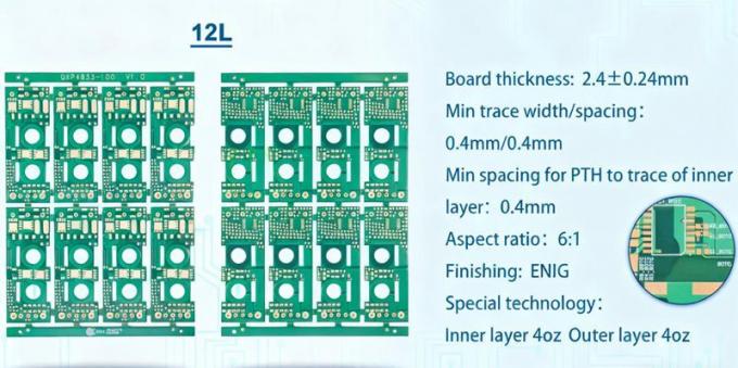
| PCB Type: | Heavy Copper PCB | Layer Count: | 2– 20 Layers |
|---|---|---|---|
| Copper Thickness: | Up To 20 Oz/ft² (700 μm) | Board Thickness: | 0.5 Mm To 5 Mm |
| Min. Trace Width/Spacing: | 0.2 Mm / 0.2 Mm (may Vary Based On Copper Weight) | Min Hole Size: | 0.25 Mm (10 Mil) |
| Copper Plating In Through Holes: | 25 μm To 75 μm | Surface Finishes: | ENIG, HASL, OSP, Immersion Tin, Immersion Silver |
| Certifications: | IPC, RoHS, UL, ISO9001, ISO14001,ISO13485,IATF16949 | Testing And Inspection: | Automated Optical Inspection (AOI), X-ray Inspection |
| Application Areas: | Automotive Electronics,Aerospace And Military Equipment,Renewable Energy | Solder Mask Types: | High-temperature Solder Masks, Peelable Masks |
| Impedance Control: | 50 Ω, 75 Ω (±5% Tolerance) |
Product Description
What Is a Copper Based PCB?
A Copper based PCB is a type of metal core printed circuit board that uses copper as the base material instead of traditional FR-4. Due to copper’s excellent thermal conductivity, this PCB structure is widely used in applications requiring efficient heat dissipation, high power density, and long-term reliability. A Copper based PCB typically consists of a copper base layer, a high-performance dielectric layer, and a copper circuit layer.
Compared with aluminum or standard FR-4 boards, Copper based PCB solutions offer superior thermal management, making them ideal for high-power and high-frequency electronic applications.
Note:
The above parameters are for reference only. Final specifications and designs depend on your project requirements.
Please contact our professional customer service team for customized solutions: rfq@ringpcb.com
Key Features and Advantages of Copper Based PCB
1. Excellent Heat Dissipation
Copper has outstanding thermal conductivity, allowing fast heat transfer from critical components. This significantly improves product stability and lifespan.
2. High Mechanical Strength
A Copper based PCB provides better mechanical rigidity and durability, suitable for harsh environments and industrial-grade applications.
3. High Current Carrying Capacity
Thanks to thick copper layers and a solid metal core, Copper based PCB designs can handle high current loads with minimal power loss.
4. Superior Reliability
Reduced thermal stress and improved heat distribution help minimize failure rates, especially in high-power LED, automotive, and power electronics.
5. Customizable Structure
Ring PCB supports full customization of Copper based PCB stack-ups, copper thickness, surface finish, and overall design to meet specific industry needs.
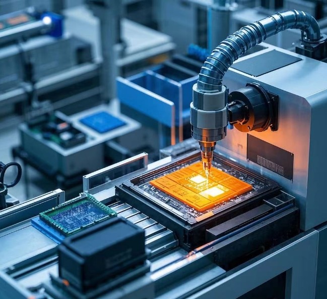
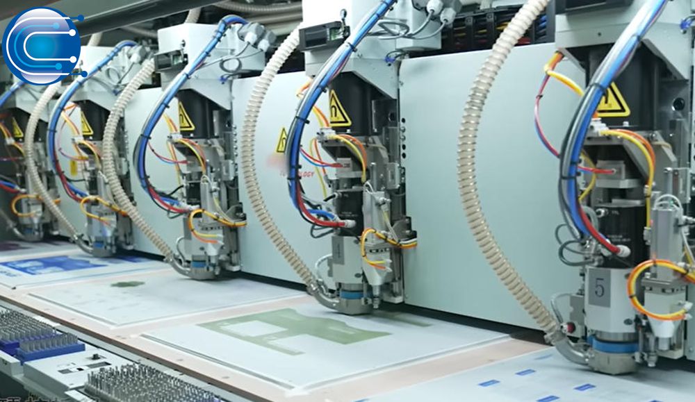
The Manufacturing Challenges for Heavy Copper PCBs at Ring PCB
1. Etching Process
Challenge: Standard PCB etching techniques struggle with thick copper layers. As copper thickness increases, the etching process becomes more difficult, requiring precise control to avoid uneven or incomplete etching.
Solution: Advanced etching processes are employed to handle thicker copper, using controlled chemical etching and temperature management to achieve uniform copper traces. In some cases, multiple etching steps are used to gradually achieve the desired thickness.
2. Thermal Management During Manufacturing
Challenge: Thick copper layers retain heat, which can lead to issues with warping, delamination, or internal stress during high-temperature processes like lamination and soldering.
Solution: Temperature control and gradual thermal cycling are applied throughout manufacturing. Special solder masks that can endure higher temperatures are also used to prevent damage during soldering and reflow.
3.Drilling and Hole Quality
Challenge: Heavy Copper PCBs are more difficult to drill accurately due to their dense copper layers, which can cause bit wear, misalignment, and burrs around drilled holes.
Solution: Ring PCB reduces lifespan of drill bits and replace them sooner. Additionally, using high-precision drilling machines and specialized drill bits designed for thick copper can be beneficial. Furthermore, segmenting the drilling process can help minimize drill bit wear.
4.Copper Plating
Challenge: Plating thick copper requires copper plating layer can adhere to the original copper layer, enhancing the overall bonding strength.
Solution: PCBs are typically subjected to cleaning to remove contaminants, followed by both chemical and mechanical roughening to create a microscopically rough surface on the copper. A final copper plating step ensures uniform coverage.
5.Hole Size Compensation
Challenge: After the copper plating in Heavy Copper PCB manufacturing, the hole size can become smaller. This is because the plating process deposits additional copper within the drilled holes, increasing the thickness of the copper on the hole walls and slightly reducing the diameter.
Solution: Ring PCB carefully calculates the initial drill size based on the thickness of copper that will be added in the plating process. The hole is drilled slightly larger than the final required size to allow for the subsequent plating buildup.
5.Applications of Heavy Copper PCBs
Heavy Copper PCBs are indispensable in applications where high current and enhanced thermal performance are essential. Some common applications include:
Automotive Electronics: Used in electric vehicles, power converters, and braking systems due to their high current handling.
Aerospace and Military Equipment: Essential for equipment where reliability and durability in extreme environments are required.
Power Supplies: Heavy Copper PCBs are ideal for uninterruptible power supplies (UPS) and other high-power devices that require stable power management.
Renewable Energy: Found in wind turbines and solar power systems, where high current capacity and durability are needed for efficient energy conversion.
Industrial Equipment: Used in heavy-duty machinery, motor controls, and power distribution units for efficient heat management and reliability.
Ring PCB supports 3-day rapid prototyping and 7-day mass production, depending on design complexity and order quantity.
One-Stop Service for PCB and PCBA Solutions!
Ring PCB’s Key Advantages
-
Advanced Engineering for Precision PCB Manufacturing
-
High-Density Stack-Up: 2-48 layer boards, ideal for 5G, industrial control, medical devices, and automotive electronics.
-
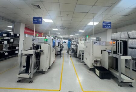
Smart Manufacturing: Self-owned facilities with LDI laser exposure, vacuum lamination, and flying probe testers, ensuring compliance with IPC-6012 Class 3 standards.
-
-
Integrated PCBA Services | One-Stop Turnkey Solutions
-
Full Assembly Support: PCB fabrication, component sourcing, SMT assembly, and functional testing, all under one roof.
-
DFM/DFA Optimization: Our expert engineering team optimizes designs to reduce risks and BOM costs, enhancing efficiency.
-
Rigorous Quality Control: X-ray inspection, AOI testing, and 100% functional validation ensure zero-defect delivery.
-
-
Self-Owned Factory with Full Supply Chain Control
-
Vertical Integration: We manage raw material procurement, production, and testing in-house, ensuring maximum control over the production process.
-
Triple Quality Assurance: AOI, impedance testing, and thermal cycling with a defect rate of <0.2% (industry average: <1%).
-
Global Certifications: ISO9001, IATF16949, and RoHS compliance to meet international standards.
-
Why Choose Ring PCB?
-
18Years of Excellence in PCB and PCBA manufacturing, offering high-quality, reliable products for critical applications.
-
Self-Owned Factories ensure full control over the production process, allowing us to meet strict deadlines and guarantee consistent quality.
-
End-to-End Technical Support: From design and prototyping to mass production and final assembly, we provide comprehensive support at every stage.
-
Fast Turnaround: Prototype production within 3 days and mass production within 7 days to keep your projects on schedule.
-
Global Reach: Serving customers in over 50 countries with ongoing industrial partnerships.
Contact Us
📧 Email: rfq@ringpcb.com