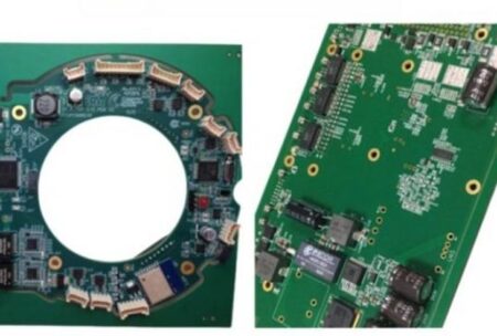
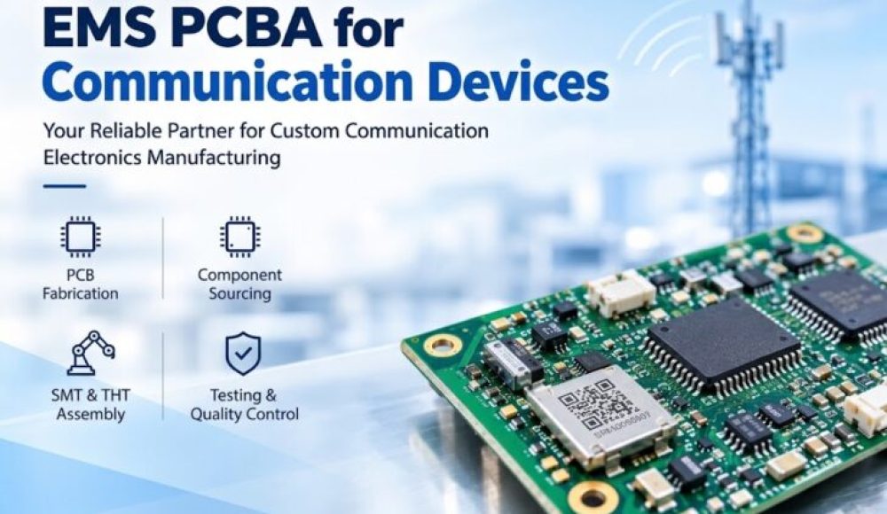
When you need EMS PCBA for a communication device, inconsistent component supply, unstable signal performance, poor assembly quality, and long production lead times can quickly increase project risk. You need a manufacturing partner that can handle PCB fabrication, component sourcing, SMT assembly, testing, and quality control within one coordinated process. Ring PCB provides customized communication PCBA manufacturing for mobile scanning terminals, data acquisition equipment, industrial signal interfaces, and other compact electronic devices.
What Is EMS PCBA for Communication Devices?
EMS PCBA combines electronic manufacturing services with professional printed circuit board assembly. Instead of managing PCB fabrication, component procurement, assembly, inspection, and testing through separate suppliers, you can use one integrated manufacturing partner.
For communication equipment, this approach is particularly useful because signal integrity, component availability, assembly precision, and testing must work together. Ring PCB supports OEM, ODM, and turnkey EMS PCBA services based on your Gerber files, BOM, drawings, and technical requirements.
Typical applications include:
- Mobile scanning terminals
- Communication interface modules
- Data acquisition equipment
- Industrial signal converters
- Portable debugging equipment
- IoT and automation devices
- Intelligent robotics electronics
Why Choose Ring PCB for Communication PCBA Manufacturing?
Ring PCB has operated in Shenzhen since 2008 and has accumulated 18 years of PCB and PCBA manufacturing experience. Its approximately 10,000-square-meter self-owned facility employs around 500 people and supports both prototype development and volume production.
The company can manufacture up to 50,000 PCBs and 500 PCBA assemblies per month, giving you flexible capacity for samples, pilot runs, and larger production requirements.
For communication equipment projects, Ring PCB provides:
- Custom irregular PCB manufacturing
- Precision SMT and selective hand soldering
- Component sourcing and supply-chain management
- AOI and X-ray inspection
- ICT and functional testing
- BGA rework
- Conformal coating
- Aging and burn-in testing
- DFM engineering support
- Custom packaging
This integrated structure helps you reduce supplier coordination and improve production traceability.
Custom Communication Device PCBA Capabilities
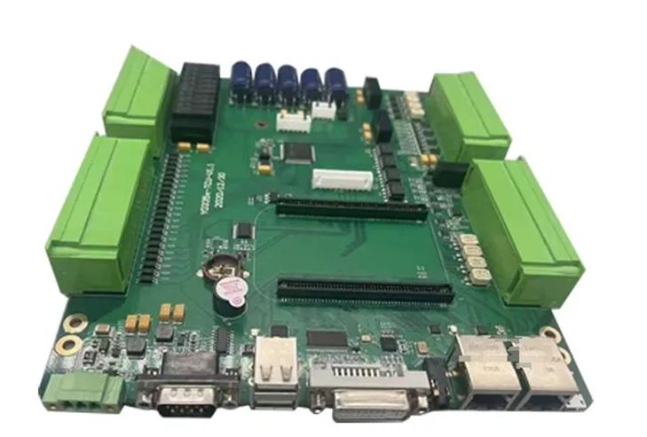
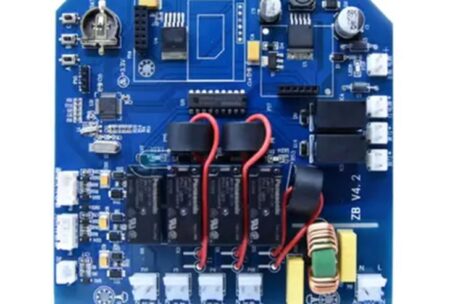
The Communication Device PCBA for Mobile Scanning Terminal is designed around a custom irregular PCB outline. Its compact structure allows the board to fit specialized portable device enclosures where a standard rectangular PCB may not be suitable.
The board supports 2-layer to 8-layer multilayer PCB configurations, with FR-4 material and ENIG, OSP, or HASL surface finishes according to project requirements.
Its main technical features include:
- MCU-based control circuitry
- Power regulation circuits
- Dedicated DATA, TCK, TDO, and GND test points
- Optimized signal routing
- Compact SMT component placement
- Signal conversion and data acquisition
- Communication interface integration
For you, these features can simplify debugging and help engineers monitor critical signals during prototype verification and production testing.
EMS PCBA vs. Conventional PCB Assembly
Choosing between a basic assembly supplier and a full EMS PCBA partner depends on how much manufacturing responsibility you want to outsource.
| Capability | Conventional PCB Assembly | Ring PCB EMS PCBA |
|---|---|---|
| PCB fabrication | Usually outsourced | Integrated |
| Component sourcing | Limited or customer supplied | Supported |
| SMT assembly | Yes | Yes |
| THT assembly | Depends on supplier | Supported |
| DFM engineering | Limited | Available |
| AOI inspection | Depends on supplier | Available |
| X-ray inspection | Depends on supplier | Available |
| Functional testing | Project dependent | Supported |
| Turnkey manufacturing | Limited | Available |
| Mass production | Varies | Supported |
Therefore, if your project requires component procurement, PCB manufacturing, assembly, testing, and production management, a turnkey EMS PCBA model can provide a more streamlined workflow.
How Ring PCB Handles a Communication PCBA Project
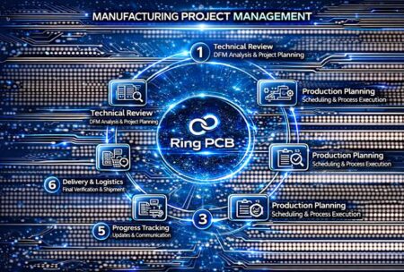
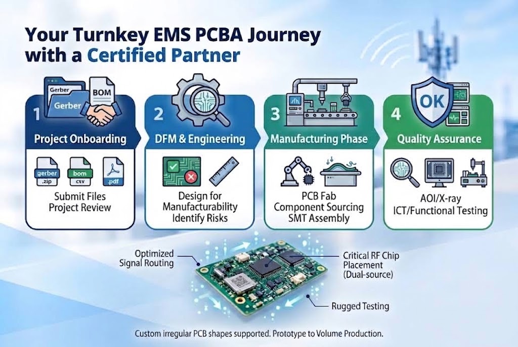
You can follow a structured process to move from design files to finished assemblies:
- Submit your project files
Provide Gerber files, BOM, drawings, specifications, and expected quantities. - Complete DFM analysis
Ring PCB engineers review manufacturability, component placement, PCB structure, and potential production risks. - Confirm components and PCB production
The team coordinates component sourcing and PCB fabrication according to your approved specifications. - Perform SMT and THT assembly
Automated production equipment mounts components with controlled soldering processes. - Inspect and test the PCBA
AOI, X-ray inspection, electrical testing, and functional testing can be applied according to your project requirements. - Complete aging and delivery preparation
Selected projects can undergo thermal, environmental, or burn-in testing before packaging and shipment.
This process gives you a clearer manufacturing path from prototype validation to repeat production.
Quality Certifications and Manufacturing Control
For communication equipment, quality management is just as important as assembly capability. Ring PCB operates according to internationally recognized management systems, including ISO9001, ISO14001, ISO13485, IATF16949, and UL certification.
The company also supports compliance requirements involving RoHS and REACH, while production inspection can include X-ray solder-joint analysis, RF signal performance testing, thermal cycling, damp-heat testing, and full-load burn-in.
Ring PCB also uses dual-source procurement for selected critical RF chips, MCUs, and connectors. This approach can reduce the risk of production delays caused by component shortages.
FAQ
1. What information do you need for a custom communication PCBA?
You can provide Gerber files, BOM, schematics, PCB drawings, technical specifications, target quantity, and testing requirements. If your design is still under development, Ring PCB can also provide DFM engineering support.
2. Can Ring PCB manufacture low-volume communication PCBA?
Yes. Ring PCB supports prototype verification, sample orders, and mass production. The stated MOQ for this communication PCBA product is 1 unit, while production quantities can scale according to project requirements.
3. How long does communication PCBA production take?
The listed delivery time for this product is 10–15 working days. Actual lead time can vary depending on PCB complexity, component availability, testing requirements, and order quantity.
Conclusion
Selecting the right EMS PCBA partner can directly affect your communication device’s production efficiency, quality consistency, and scalability. With 18 years of manufacturing experience, a 10,000-square-meter facility, approximately 500 employees, monthly capacity of up to 50,000 PCBs and 500 PCBA assemblies, and certifications including ISO9001, ISO13485, IATF16949, and UL, Ring PCB provides a structured solution for custom communication electronics.
Request a communication PCBA quote from Ring PCB today. Send your Gerber files, BOM, drawings, target quantity, and testing requirements to receive a customized manufacturing assessment and production solution.