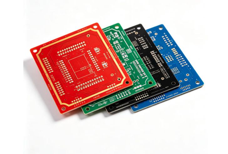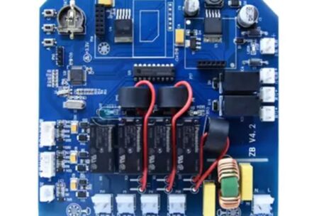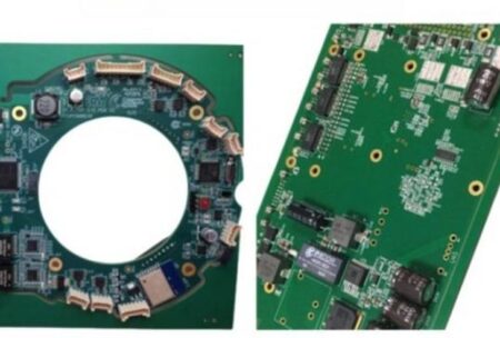
The rapid expansion of AI servers, high-speed communication hardware and industrial control electronics has pushed multilayer PCBs into a high-growth era in 2026. Unlike simple double-sided boards, multilayer PCBs integrate multiple conductive and insulating layers to achieve dense routing, stable power delivery and high-speed signal transmission. As electronic products become more compact and powerful, hardware engineers and procurement managers must understand manufacturing bottlenecks before selecting suppliers.
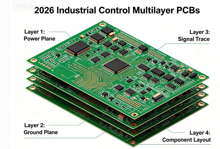
What Makes Multilayer PCBs Manufacturing Technically Demanding
First of all, interlayer alignment control stands as the biggest hurdle. Each additional layer multiplies the risk of registration deviation. For high-layer PCBs, even tiny misalignment will trigger open circuits, short circuits or impedance drift, which can completely invalidate high-speed designs. Secondly, lamination process needs precise temperature and pressure control. Improper parameters easily cause delamination, bubbles or board warpage. Moreover, deep-hole plating is a persistent pain point. High-aspect-ratio vias in thick multilayer boards require stable copper deposition inside hole walls, otherwise thermal cycling will crack via barrels and cause field failure.
Many electronics teams underestimate these technical risks. A design perfect in simulation may end up with low yield if the manufacturer lacks advanced lamination, laser drilling and AOI inspection equipment. For boards above 24 layers, process experience becomes far more important than simple production capacity.
Key B2B Buyer Criteria When Evaluating Multilayer PCB Suppliers
When you source multilayer PCBs, raw price comparison is never enough. Here are four core points every procurement team should verify.
- Maximum layer capability. Standard factories handle 4–16 layers smoothly, yet only mature manufacturers can reliably fabricate boards above 40 layers. This capability directly decides whether your complex server or test board project can move forward.
- In-house full production line. Outsourcing key procedures such as inner layer imaging or plating will create quality blind spots and delay delivery.
- First-pass yield data and IPC compliance. Confirm if the supplier can provide cross-section reports, impedance test records and full traceability.
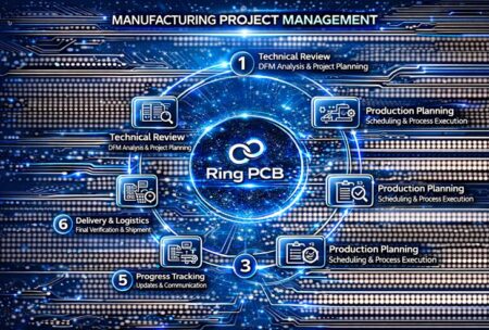
- Engineering DFM support. Early design review helps reduce revision costs and shorten lead times. Many failures occur because manufacturers start production without DFM feedback.
Why One-Stop PCB & PCBA Service Adds Extra Value
A multilayer bare board is only half the project. If you separate PCB fabrication and PCBA assembly between two vendors, troubleshooting defects becomes complicated. When finished assemblies malfunction, you will spend weeks identifying whether the problem comes from bare board fabrication or soldering. A one-stop PCB & PCBA manufacturer unifies bare board production, component mounting and final electrical testing under one roof. Single-point accountability eliminates cross-supplier blame and cuts hidden management costs.

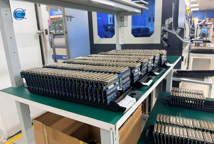
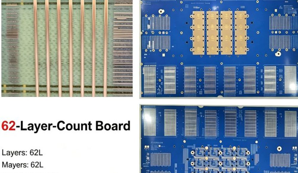
For complex multilayer projects, Ring PCB acts as a trusted one-stop PCB & PCBA manufacturer with 18 years of manufacturing expertise. Our multilayer PCBs manufacturing capability reaches up to 62 layers, perfectly matching high-speed server and semiconductor test board demands. Our monthly bare PCB production capacity hits 50,000 ㎡, and we can manage up to 500 PCBA projects monthly to serve prototype and mixed small-to-medium batch orders. Our full-range workshop equipment and strict in-house QC processes keep consistent quality for projects of varying complexity. Our engineering team also provides professional DFM review before production to avoid unnecessary design revisions.
If you are preparing a multilayer PCB or integrated PCBA project and want a detailed technical review and quotation, send your Gerber and BOM files to rfq@ringpcb.com.