HDI PCB Manufacturer: Choosing the Right Microvia Technology
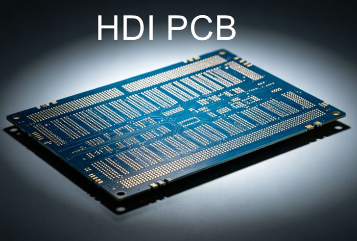
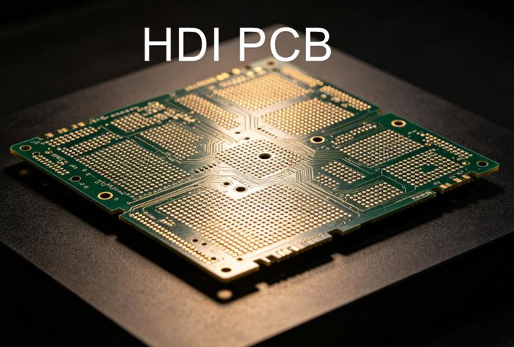
High-density interconnect (HDI) PCBs help electronic manufacturers fit more electrical connections into smaller board areas. By using fine traces, compact component layouts, and microvia structures, HDI technology supports products that require high routing density without continuously increasing board dimensions.
For OEMs developing compact industrial electronics, communication equipment, automotive electronics, and computing hardware, choosing the right HDI PCB manufacturer is an important engineering decision. The supplier must understand not only fine-line fabrication but also build-up structures, microvia processing, registration, and the requirements of the finished assembly.
Why HDI PCB Technology Matters
Modern electronic components increasingly combine high pin counts with compact package dimensions. Conventional through-hole routing may not provide enough routing space for every design, particularly around fine-pitch BGAs.
HDI construction can create additional routing channels through sequential build-up layers and laser-drilled microvias. This helps engineers connect dense component footprints while controlling board size.
Market research also reflects growing demand for advanced interconnect technology. A 2026 industry outlook from ICAPE Group, referencing Prismark estimates, projects continued growth in HDI and high-layer-count PCB demand, with AI and data-center electronics among the important drivers. These forecasts are estimates rather than guarantees, but they highlight why HDI manufacturing capability matters to product developers. <Cite refs={[“turn775088search35”]}/>
Understand the Different HDI Build-Up Structures
Not every HDI project requires the most complex structure.
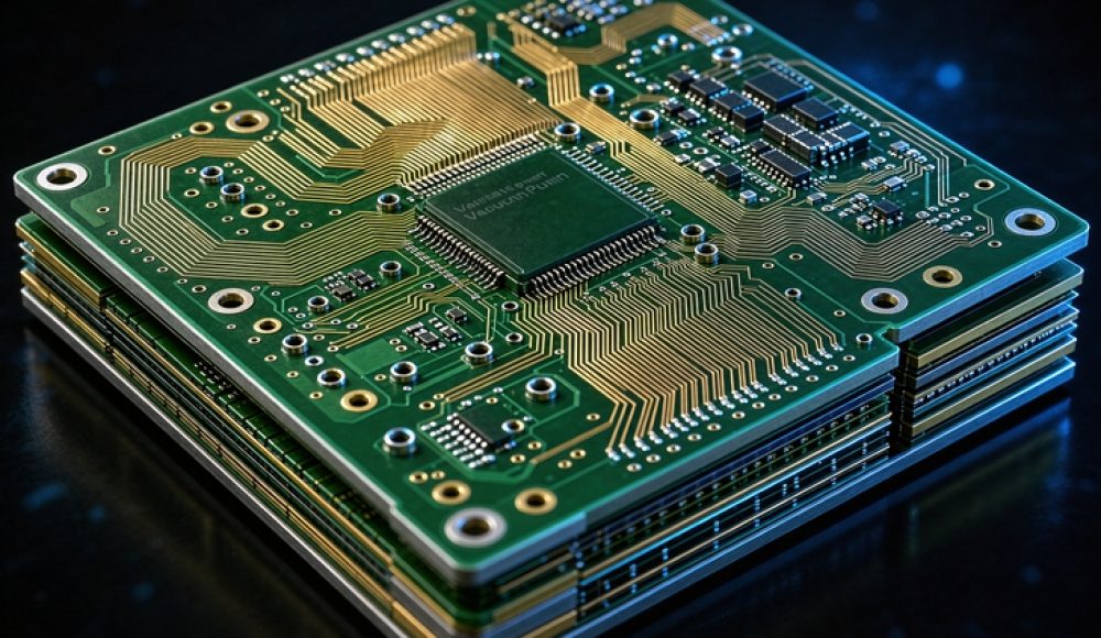
A single build-up design may be sufficient when only one additional routing layer is needed on each side of a core. More complex designs can require multiple build-up layers, buried vias, or stacked and staggered microvias.
The correct construction depends on component pitch, routing density, electrical requirements, board thickness, and cost targets.
Before selecting an HDI PCB manufacturer, provide the proposed layer structure and identify critical components. The supplier can then assess whether the microvia arrangement and layer sequence are suitable for fabrication.
Choosing a more advanced HDI structure than necessary can increase processing steps and cost. Therefore, engineering feasibility should be evaluated alongside routing benefits.
Evaluate Microvia and Via-in-Pad Requirements
Microvias connect adjacent or nearby layers and are commonly produced using laser drilling. Their dimensions and geometry influence the manufacturing process and the available routing space.
Via-in-pad structures can help escape fine-pitch components by placing a via directly within a component pad. However, they may require via filling, planarization, and additional plating processes to create a suitable surface for assembly.
Stacked microvias also require careful alignment and process control. The appropriate structure should be determined by the design requirements and the manufacturer’s validated capabilities.
OEMs should confirm microvia dimensions, aspect ratios, filling requirements, and applicable inspection criteria before releasing production files.
Review Fine-Line Fabrication Capability
HDI manufacturing relies on precise imaging and etching to produce narrow traces and spaces.
As line widths decrease, small variations in imaging, copper thickness, and etching can have a greater impact on the finished geometry.
When requesting a quotation, customers should provide their minimum trace and space requirements rather than relying on a general statement that a supplier supports HDI.
The manufacturer should evaluate the actual copper weight, layer position, finished dimensions, and production quantity. These details help determine whether the proposed design is practical and what tolerances can be supported.
Consider Assembly Requirements at the Same Time
HDI PCB fabrication and PCBA should not be treated as completely separate decisions.
Fine-pitch BGAs, small passive components, and dense layouts can introduce assembly challenges. Pad geometry, solder mask design, component placement, and board flatness can all influence downstream manufacturing.
If the final product requires SMT assembly, share the assembly drawings and relevant component information during the engineering review.
A supplier that coordinates PCB fabrication with assembly can help identify potential manufacturing conflicts before the boards enter production.
Ask About Quality Verification and Documentation
HDI boards may contain internal connections that are not visible through ordinary surface inspection.
Depending on the construction and customer specification, verification can include electrical testing, dimensional inspection, and additional checks for specialized via structures.
OEMs should establish acceptance requirements before production. If the design requires microvia reliability qualification or particular test methods, those requirements should be explicitly agreed upon rather than assumed.
The supplier should also maintain clear revision control so that fabrication data, stackup details, and approved changes remain aligned.
How Ring PCB Supports HDI Projects
Established in 2008, Ring PCB provides PCB fabrication, component sourcing, SMT and through-hole assembly, and full-turnkey PCBA services. Its published manufacturing capabilities include multilayer boards up to 62 layers, supporting projects with complex interconnection requirements.
For an HDI project, customers can submit Gerber files, stackup information, drill data, material specifications, and target quantities for a manufacturing review.
Ring PCB also offers PCB prototyping in as little as 3 days for qualifying projects. Actual lead times depend on the HDI structure, material availability, process requirements, and order conditions.
When selecting an HDI PCB manufacturer, look beyond the minimum feature size. Microvia capability, build-up experience, assembly coordination, quality requirements, and engineering communication all contribute to a successful project.
To discuss your HDI PCB requirements, contact rfq@ringpcb.com.
References
- ICAPE Group. Global PCB Report: Industry Insights, Q4 2025.
- IPC. IPC-2226, Sectional Design Standard for High Density Interconnect (HDI) Printed Boards.