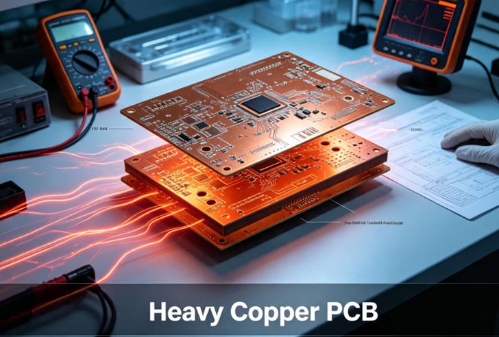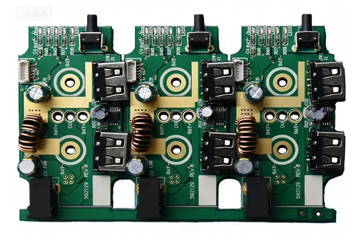
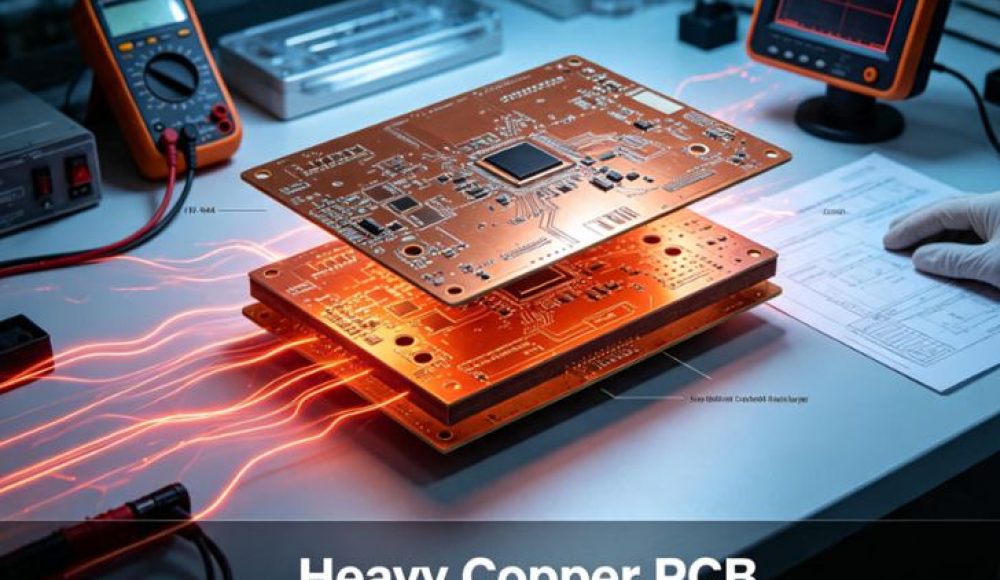
Heavy copper PCBs are used in electronic systems that require high current capacity, improved heat spreading, or robust copper conductors. Typical applications include power supplies, industrial motor drives, energy conversion equipment, battery systems, and selected automotive electronics.
However, increasing copper thickness does not automatically solve every electrical or thermal problem. It also changes etching behavior, trace geometry, board weight, and manufacturing requirements.
For OEM engineers, the challenge is to balance electrical performance with thermal management, manufacturability, and total project cost.
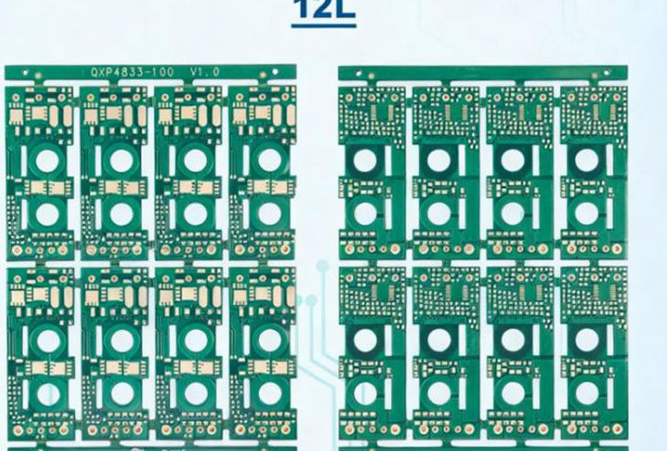
What Makes a PCB a Heavy Copper PCB?
Heavy copper PCBs use thicker copper layers than many conventional circuit boards. The required copper thickness depends on the application and the manufacturer’s process capability.
Thicker copper can reduce conductor resistance and help carry higher currents. It can also support power distribution and heat spreading in appropriately designed structures.
Nevertheless, the finished board must be evaluated as a complete system. Current capacity depends on conductor width, copper thickness, allowable temperature rise, surrounding materials, airflow, and operating conditions.
Therefore, specifying copper thickness alone is not enough to establish a board’s electrical capability.
Calculate Current and Temperature Rise Together
When current flows through a copper trace, electrical resistance generates heat. Increasing copper cross-sectional area can reduce resistance, but the resulting temperature also depends on how effectively the heat can escape.
Engineers should consider continuous current, peak current, duty cycle, ambient temperature, and acceptable temperature rise.
For example, a power conversion board operating continuously inside an enclosed cabinet may face different thermal constraints from a board exposed to substantial airflow.
The trace geometry and surrounding copper planes also affect heat distribution.
Rather than relying on a generic current rating, OEMs should define the actual operating conditions and evaluate the design accordingly. Applicable design guidance and thermal calculations can then help establish a reasonable starting point for verification.
Balance Copper Thickness With Trace Width
Increasing copper thickness may allow a conductor to carry more current without increasing its width by the same proportion.
However, thick copper can be more challenging to pattern accurately. Etching removes copper laterally as well as vertically, and this can influence the finished trace profile.
As a result, narrow traces combined with very thick copper may be difficult or costly to manufacture.
For this reason, heavy copper PCB design should consider both the required current and the achievable trace geometry.
In some cases, a wider conductor or a different layer allocation may be more practical than increasing copper thickness across the entire board.
The manufacturer should review these trade-offs before the design is finalized.
Use Copper Planes and Thermal Paths Effectively
Power and ground planes can distribute current across a larger copper area and support heat spreading.
However, plane layout must also accommodate clearances, signal routing, component placement, and electrical isolation.
Thermal vias may help transfer heat between layers, while appropriate component placement can reduce localized heating.
For power electronics, the thermal path extends beyond the PCB itself. Heat sinks, enclosures, interfaces, and airflow may all affect the final operating temperature.
Therefore, heavy copper should be selected as part of a broader thermal design strategy, not as a substitute for system-level thermal analysis.
Understand the Manufacturing Challenges
Heavy copper fabrication can require adjustments to imaging, etching, plating, and lamination processes.
Thicker copper can affect fine-feature definition and the relationship between conductor geometry and insulation spacing. Copper distribution across the panel may also influence process uniformity.
When several copper thicknesses are combined within one board, the construction may require additional engineering review.
OEMs should provide the copper weight required for each layer, finished board thickness, minimum trace and space, and any special thermal or electrical requirements.
The PCB manufacturer can then assess whether the design is compatible with its production processes and identify potential cost drivers.
Consider Insulation and Operating Environment
High-current applications may expose a PCB to elevated temperatures, voltage stress, vibration, or environmental contamination.
Copper thickness alone does not determine electrical insulation performance.
Clearance, creepage, dielectric properties, solder mask requirements, board material, and operating environment must be evaluated against the applicable product requirements.
For example, a power supply used in an industrial cabinet may have different insulation and environmental requirements from a low-voltage control board.
The OEM should communicate the intended operating conditions and applicable standards before manufacturing begins.
Prepare a Complete Heavy Copper PCB RFQ
A useful quotation package should include the Gerber files, layer stackup, copper thickness by layer, finished board dimensions, material specifications, and surface finish.
Customers should also identify expected current levels, thermal constraints, insulation requirements, production quantity, and target delivery date.
If PCBA is required, include the BOM and assembly data so the supplier can consider component placement and downstream processing.
This information helps the manufacturer assess feasibility and quote the actual project rather than a generic board configuration.
Heavy Copper PCB Manufacturing With Ring PCB
Ring PCB was established in 2008 and provides PCB fabrication, component sourcing, SMT and through-hole assembly, and full-turnkey PCBA services. Its multilayer PCB capability extends up to 62 layers, while heavy copper requirements should be assessed against the specific copper thickness and design geometry requested.
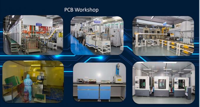
For project evaluation, customers can submit fabrication data, copper specifications, current requirements, and quantities for review.
Ring PCB offers PCB prototyping in 3 days and qualifying PCB/PCBA production schedules as short as 7 days. Actual timing depends on copper thickness, board construction, material availability, inspection requirements, and order conditions.
A well-planned heavy copper PCB balances current capacity, temperature rise, insulation, trace geometry, and manufacturing feasibility. Reviewing these factors early can help OEMs reduce redesign risk and obtain a more accurate quotation.
For your heavy copper PCB project, contact rfq@ringpcb.com.
References
- IPC. IPC-2221, Generic Standard on Printed Board Design.
- IPC. IPC-6012, Qualification and Performance Specification for Rigid Printed Boards.
- Ring PCB. https://www.ringpcb.com/