
High speed PCB manufacturing requires careful coordination between electrical performance and physical board construction. As digital signals operate at higher frequencies and faster edge rates, signal loss through PCB conductors and dielectric materials becomes an important design consideration.
For networking equipment, high-performance computing, communication systems, and advanced industrial electronics, excessive insertion loss can reduce signal amplitude and limit the available signal-integrity margin.
However, selecting a material with a low published loss value is not enough. OEMs must consider the complete transmission path, including laminate properties, copper characteristics, trace geometry, vias, connectors, and manufacturing tolerances.

What Is Insertion Loss in a High Speed PCB?
Insertion loss describes the reduction in signal power as a signal travels through an interconnection.
In PCB transmission lines, loss can result from conductor resistance and dielectric dissipation. At higher frequencies, current distribution within the copper changes, while dielectric materials absorb part of the signal energy.
The impact depends on signal frequency, trace length, conductor geometry, and the properties of the materials used.
For example, a short connection may tolerate a material choice that becomes unsuitable when the same signal must travel across a much longer board.
Therefore, engineers should evaluate insertion loss against the actual signal path rather than choosing a laminate based on a single headline specification.
Match Laminate Properties to the Application
Two important laminate characteristics are dielectric constant, often expressed as Dk, and dissipation factor, commonly expressed as Df.
Dk influences signal propagation and transmission-line impedance. Df indicates the degree of dielectric energy loss under specified measurement conditions.
For high-speed designs, engineers should review these properties at relevant frequencies and under conditions appropriate to the application.
Material data should also be considered alongside thermal performance, dimensional stability, moisture behavior, and processing compatibility.
IPC-4103 addresses base materials for high-speed and high-frequency printed-board applications, including requirements relating to dielectric properties. It provides a useful reference when evaluating suitable laminate specifications.
Nevertheless, no single material is optimal for every project. The best choice depends on the required electrical performance, board construction, manufacturing feasibility, and overall cost.
Understand Copper-Related Signal Loss
Conductor loss is another important factor in high-speed PCB manufacturing.
At higher frequencies, current tends to concentrate closer to the conductor surface. This behavior, commonly associated with skin effect, increases the importance of conductor geometry and copper surface characteristics.
Copper foil roughness can also influence signal attenuation because high-frequency current interacts with the conductor surface.
For this reason, copper selection should not be based on nominal thickness alone.
Engineers should consider the copper type and roughness characteristics supported by the chosen laminate system, together with trace geometry and fabrication requirements.
The appropriate balance depends on the signal-frequency range and the board’s electrical performance targets.
Treat Trace Geometry and Stackup as One System
Insertion loss cannot be managed through material selection alone.
Trace width, copper thickness, dielectric spacing, and reference-plane configuration influence impedance and electromagnetic behavior.
If a high-speed trace must cross several board regions, changes in geometry or reference structure can introduce additional discontinuities.
The engineering team should therefore evaluate the complete signal path and identify where transitions, connectors, vias, or changes in layer routing occur.
The stackup should be reviewed early enough to avoid unnecessary changes after fabrication files have been released.
For demanding designs, simulation and engineering review can help identify potential problems before manufacturing. The resulting requirements should then be translated into clear fabrication specifications.
Account for Vias and Interconnect Transitions
A signal does not always remain on one copper layer.
Layer changes may require vias, and transitions can introduce parasitic capacitance, inductance, and impedance discontinuities.
These effects can influence insertion loss and return loss, particularly as operating frequencies increase.
Design teams should evaluate via geometry, reference-plane continuity, and the need for specialized structures according to the signal requirements.
Backdrilling or other advanced processes may be relevant to certain designs, but they should not be treated as universal requirements.
The manufacturing supplier needs enough information to determine whether the proposed interconnect structure is feasible and what process controls are necessary.
Define Measurable Acceptance Criteria
A useful high-speed PCB specification should identify the performance that must be achieved.
Depending on the design, requirements may include impedance targets, tolerances, test coupon structures, and insertion-loss limits over a defined frequency range.
It is important to distinguish between calculated design targets and verified manufacturing results.
A material datasheet describes material properties under specified conditions; it does not by itself guarantee the insertion loss of the completed PCB.
Where electrical verification is required, the customer and manufacturer should agree on suitable test methods, test structures, frequency ranges, and acceptance limits.
This makes supplier quotations more comparable and reduces ambiguity during quality review.
Coordinate PCB Fabrication With Assembly
PCB performance must be maintained through the full manufacturing process.
The chosen material and board construction should be compatible with the intended assembly process and operating environment.
For example, a high-speed board containing dense components may require careful coordination between fabrication tolerances, component footprints, and assembly requirements.
When PCBA is included, the OEM should communicate material specifications and critical electrical requirements to the manufacturing team before production.
Changes to the stackup or laminate should be reviewed for their possible effects on impedance and signal loss.
High Speed PCB Manufacturing With Ring PCB
Ring PCB provides PCB fabrication and PCBA manufacturing services, including multilayer PCB production and controlled-impedance requirements. The company was established in 2008 and reports the capability to manufacture multilayer boards up to 62 layers.
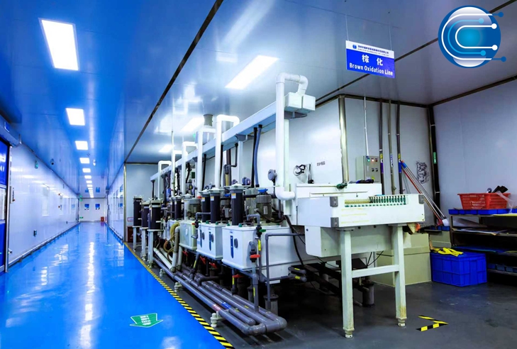
For high-speed projects, customers can submit their stackup, Gerber files, impedance requirements, material specifications, and target frequency range for project-specific review.
Ring PCB also offers PCB prototyping in as little as 3 days for qualifying designs, helping engineering teams evaluate manufacturing feasibility and prepare development builds. Actual schedules depend on the board construction, material availability, and agreed scope.
Selecting a high-speed PCB manufacturing partner means assessing whether electrical targets can be translated into practical fabrication requirements. Material selection, copper characteristics, geometry, interconnect transitions, and verification should all be considered together.
For assistance with a high-speed PCB project, contact rfq@ringpcb.com.
References
- IPC. IPC-4103, Specification for Base Materials for High Speed/High Frequency Applications.
- Ring PCB. About Ring PCB. https://www.ringpcb.com/about-us/