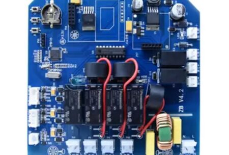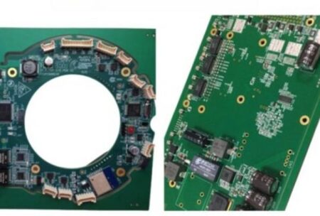
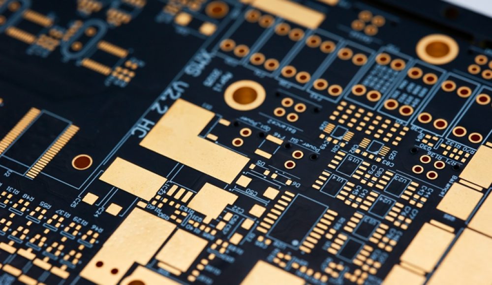
Power electronics are becoming more demanding as equipment manufacturers develop higher-capacity energy systems, electric vehicle components, industrial motor drives, and renewable energy solutions. These applications require printed circuit boards to carry substantial current while maintaining acceptable temperatures and long-term reliability.
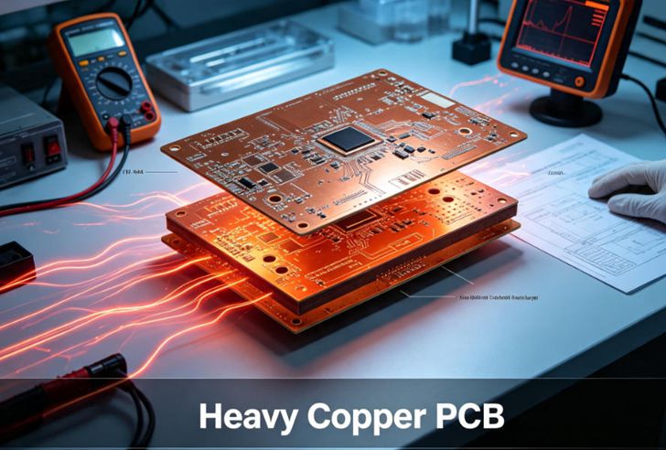
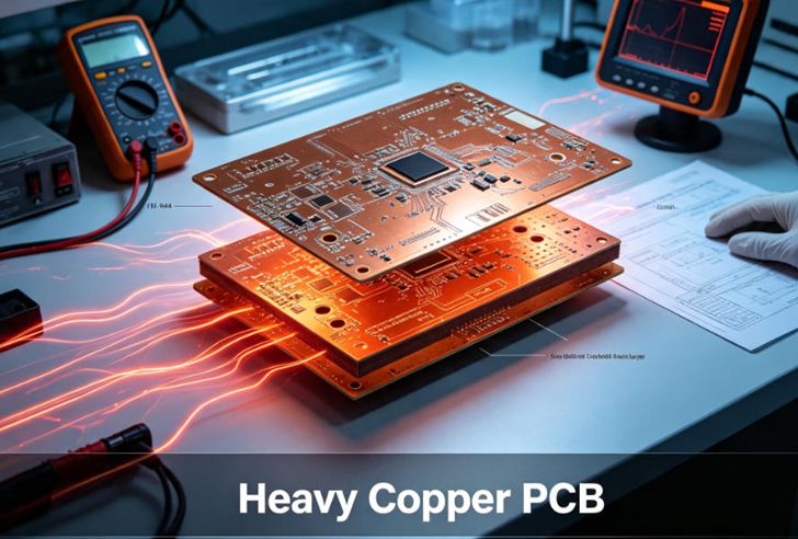
A Heavy Copper PCB can help address these requirements by using thicker copper layers to create larger conductor cross-sections. Compared with standard copper constructions, heavy copper boards can support higher current paths, reduce conductor resistance, and improve heat spreading in suitable applications.
However, simply increasing copper thickness does not guarantee a reliable power board. Trace width, spacing, thermal paths, via structures, material selection, and manufacturing limitations must all be considered together.
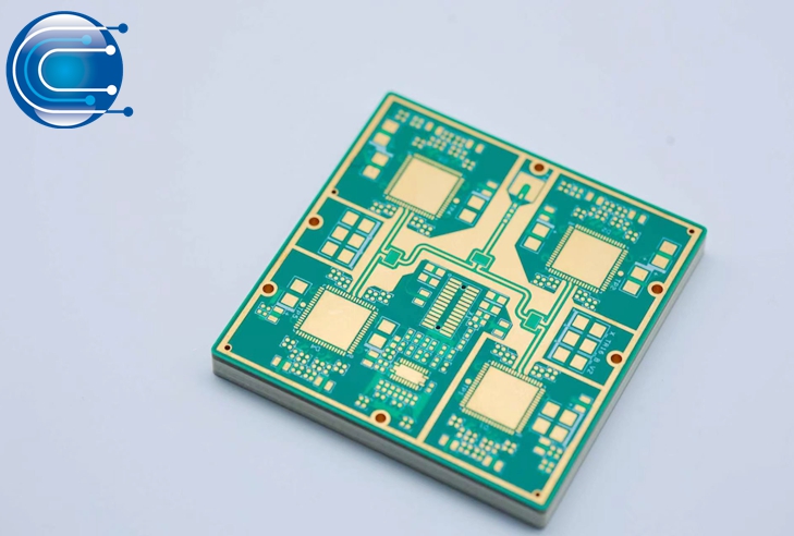
1. What Is a Heavy Copper PCB?
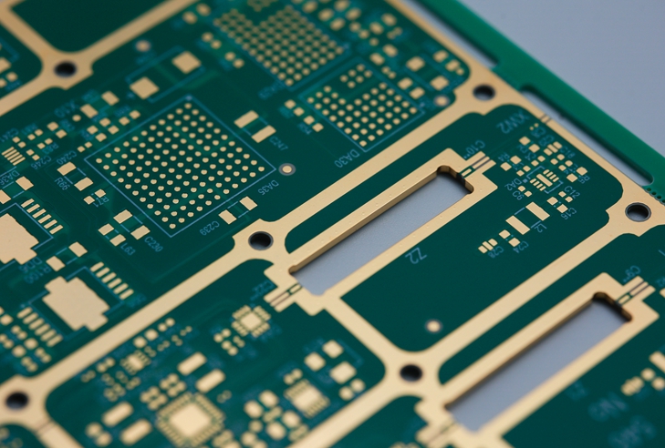
A heavy copper PCB is a printed circuit board that uses copper layers thicker than those commonly found in standard PCB constructions. In industry usage, copper weights of 3 oz/ft² or above are often described as heavy copper, although definitions and manufacturer capability ranges may vary.
For reference, approximate copper thicknesses are:
- 1 oz/ft²: 35 μm
- 2 oz/ft²: 70 μm
- 3 oz/ft²: 105 μm
- 4 oz/ft²: 140 μm
- 6 oz/ft²: 210 μm
The actual finished copper thickness may differ from the nominal starting foil weight because plating and etching processes affect the final conductor structure.
Heavy copper is commonly considered for power distribution, motor control, industrial power supplies, battery systems, and other applications where current capacity and thermal behavior are important.
Nevertheless, not every power PCB needs heavy copper. Wider traces, parallel copper layers, busbars, or alternative conductor structures may sometimes provide a more economical solution.
2. Why Are Heavy Copper Applications Becoming More Important?
The growth of electrification and power conversion is increasing the demands placed on PCB power paths.
Electric vehicle systems use power electronics for battery management, charging, motor control, and DC-DC conversion. Renewable energy equipment relies on power conversion and distribution circuits in solar inverters, energy storage systems, and related control equipment. Industrial automation also uses motor drives and power supplies that must operate reliably under continuous or variable loads.
These applications create engineering challenges involving current density, heat generation, conductor resistance, and operating temperature.
The wider PCB market is also seeing a shift toward more specialized constructions. While high-density interconnect and high-layer-count boards are receiving attention from AI and computing markets, power electronics continue to require solutions that can manage current and heat. The two trends are not identical: HDI focuses on routing density, whereas heavy copper focuses primarily on conductor cross-section and power handling.
For OEMs, the important consideration is to match the copper construction to the electrical load and thermal environment of the actual product.
3. How Copper Thickness Affects Current Capacity
Copper thickness is one of the factors that determine the resistance of a PCB conductor.
For a given conductor length and width, increasing copper thickness increases its cross-sectional area. This generally reduces DC resistance and can reduce resistive power loss at a given current.
However, current capacity cannot be determined from copper weight alone.
The result also depends on:
- Trace width and length
- Copper thickness and finished plating
- Allowable temperature rise
- Board thickness and material properties
- Internal or external layer location
- Airflow and surrounding thermal conditions
- Nearby heat-generating components
IPC-2152 is an important industry reference for evaluating current-carrying capacity in PCB conductors. It provides a more comprehensive basis for current and temperature-rise considerations than relying on a simple copper-weight chart.
For this reason, buyers should provide the manufacturer’s electrical requirements, including expected current, conductor length, available trace width, and allowable temperature rise. The manufacturer and design team can then review whether heavier copper is necessary or whether a different conductor geometry would be more practical.
4. Heavy Copper Does Not Replace Thermal Design
A common misunderstanding is that thicker copper automatically solves overheating problems.
Heavy copper can reduce conductor resistance and help spread heat across the board. However, the complete thermal path still includes components, solder joints, PCB materials, vias, heatsinks, and the surrounding environment.
For example, a power semiconductor may generate substantial heat at its package. Increasing copper thickness around the component can help distribute heat, but it cannot compensate for an inadequate heatsink interface or insufficient airflow.
Thermal performance should therefore be evaluated at the system level.
Before choosing a copper weight, consider:
- The heat generated by each power component.
- The temperature limits of the components and PCB materials.
- The thermal path from the component to the board and heatsink.
- The location and density of thermal vias.
- The enclosure, airflow, and ambient temperature.
- The expected operating duty cycle.
Thermal simulation, engineering calculations, and prototype measurements may all contribute to validation. The appropriate method depends on the product’s complexity and risk level.
5. Manufacturing Challenges: Etching, Plating, and Spacing
Heavy copper boards require process adjustments compared with many standard PCB constructions.
One challenge is etching. Thicker copper takes more process control to form the required conductor geometry. As copper thickness increases, maintaining narrow spacing and fine trace details can become more difficult. Over-etching, under-etching, and uneven conductor profiles can affect the finished circuit.
Plating is another important consideration. The manufacturer must control copper deposition and finished conductor dimensions according to the specified construction. Thick copper features can also affect the board’s surface profile and subsequent solder mask application.
Drilling and hole plating may require additional attention, especially when the board combines thick copper layers with demanding hole structures or high aspect ratios.
These challenges create a practical trade-off between copper thickness and routing density. A design that combines very heavy copper with extremely narrow spacing may be difficult or costly to manufacture.
Buyers should therefore discuss minimum spacing, trace geometry, board thickness, drill requirements, and finished copper targets with the manufacturer before finalizing the production data.
6. Choose the Right Copper Weight for the Application
More copper is not always better. Excessive copper thickness can increase material and processing costs, reduce routing flexibility, and complicate lamination or etching.
The appropriate copper weight should be selected based on electrical and thermal requirements rather than a general preference for thicker conductors.
For example:
- Industrial power supplies may use thicker copper in selected power distribution layers.
- Motor drives may require robust current paths for switching and motor output circuits.
- Battery-related power boards may need carefully designed high-current connections.
- Renewable energy conversion equipment may use heavy copper in selected areas to support power distribution.
- Welding and other high-current equipment may require specialized conductor structures beyond ordinary PCB copper weights.
In some designs, a hybrid stackup may be considered, using heavier copper on power layers and thinner copper on signal layers. This can help balance current capacity with routing requirements, but it requires careful review of lamination, etching, and electrical performance.
7. How Heavy Copper Affects PCB Cost and Lead Time
Heavy copper PCBs can cost more than standard constructions, but the premium is not determined by raw copper price alone.
Manufacturing complexity is a major factor. Additional etching control, plating requirements, material selection, inspection, and lower panel utilization may influence the final quotation.
The board’s design also matters. A relatively simple power board with wide conductor spacing may be easier to manufacture than a dense design combining thick copper with fine features, complex drilling, and multiple layers.
Lead time can also be affected by material availability, production scheduling, process complexity, and inspection requirements.
To obtain a more accurate quotation, buyers should provide:
- Required copper weight for each layer
- Finished copper thickness requirements
- Board dimensions and thickness
- Trace width and spacing
- Current and temperature-rise requirements
- Hole and via specifications
- Surface finish and solder mask requirements
- Expected order quantity and delivery schedule
Providing these details early helps the manufacturer identify process limitations and clarify the cost implications before production.
8. What Should OEMs Confirm Before Ordering?
A structured review can help reduce manufacturing risk.
First, confirm the actual current requirements and allowable temperature rise. Next, review whether the selected copper weight and trace geometry are appropriate for the load. Then confirm the manufacturer’s process capability for the specified copper thickness, spacing, drilling, plating, and board construction.
Quality expectations should also be agreed in advance. Depending on the application, buyers may require dimensional inspection, electrical testing, visual inspection, and additional thermal or reliability validation.
For long-life industrial or power electronics products, repeat-order consistency is equally important. Changes to materials, copper construction, or process conditions should be reviewed through an agreed change-control process.
Working with Ring PCB
For projects requiring rigid PCB fabrication and PCBA manufacturing, Ring PCB provides PCB fabrication, component sourcing, SMT assembly, through-hole assembly, and production quality inspection. Established in 2008, the company operates a self-owned manufacturing facility covering more than 10,000 square meters and supports rigid PCB manufacturing of up to 62 layers.
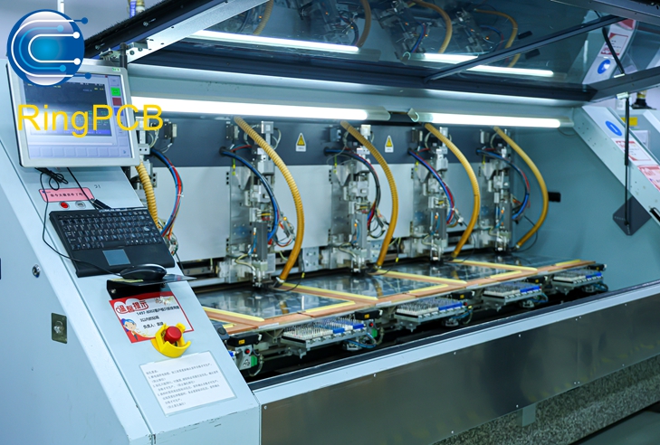
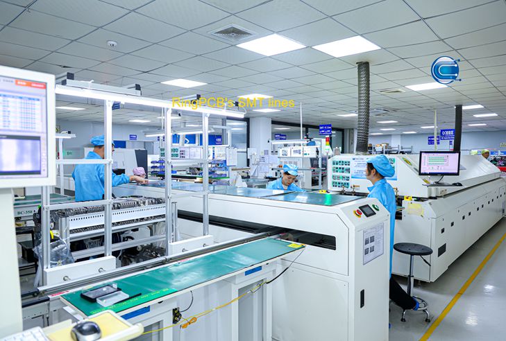
Ring PCB also operates five automated SMT production lines and uses first article inspection equipment to support production verification. Prototype lead times may be as short as 72 hours, depending on project requirements, material availability, and production conditions.
Customers can submit Gerber files, BOM information, and technical specifications for manufacturing communication and feasibility review. For heavy copper projects, the required copper weight, spacing, conductor geometry, and process conditions should be confirmed against the specific manufacturing scope before an order is accepted.
For PCB fabrication and PCBA inquiries, contact:
References and Sources
- IPC — IPC-2152: Standard for Determining Current-Carrying Capacity in Printed Board Design
- HLCPCB — Heavy Copper PCB: Copper Weight, DFM and Current-Path Review, August 2026
- PCBark — Heavy Copper PCB: The Complete Engineering Guide, 2026
- Ring PCB — Company manufacturing information, www.ringpcb.com