High-power supplies are essential to industrial automation, telecommunications, renewable energy systems, data centers, medical equipment, and many other electronic applications. As power density increases, power supply assemblies must deliver stable electrical performance while managing heat, switching noise, mechanical stress, and demanding operating conditions.
A high power supply PCBA is not simply a standard circuit board populated with larger components. Its performance depends on the interaction between PCB construction, power semiconductor selection, copper geometry, component placement, soldering quality, and thermal design.
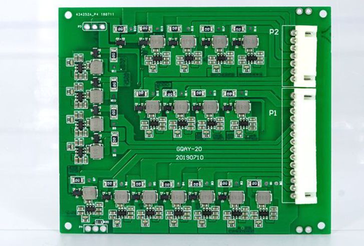
For OEMs and power electronics manufacturers, these factors make the choice of PCB assembly partner an important part of product development and production planning.
This article explores the major manufacturing considerations for high power supply PCBAs, from PCB material and copper requirements to component assembly and production quality control.
1. Understanding High Power Supply PCBA Applications
High-power supply assemblies are used in a wide range of products. Although their electrical architectures differ, many share the need for efficient power conversion and stable operation under load.
Typical applications include:
- Industrial AC/DC power supplies
- DC/DC converter modules
- Telecom rectifier systems
- Server and data-center power supplies
- Renewable energy conversion equipment
- Battery charging systems
- Motor drive and control power units
- High-power LED drivers
Depending on the application, a power supply PCBA may include switching controllers, MOSFETs, IGBTs, SiC or GaN devices, rectifiers, transformers, inductors, capacitors, current sensors, and protection circuits.
The assembly requirements depend on the electrical topology, voltage and current ranges, switching frequency, cooling arrangement, and intended operating environment.
2. PCB Copper Design and Current-Carrying Capacity
Copper structure is one of the most important factors in high-current PCB design.
A conductor’s resistance depends on its length, cross-sectional area, and material properties. For a given current, excessive resistance can increase power dissipation and temperature rise. Therefore, trace width, copper thickness, current path, and connection geometry should be evaluated together.
Heavy copper PCB construction can support high-current applications by providing a larger copper cross-section. It may also help spread heat across the board, depending on the layout and cooling conditions.
However, using heavier copper introduces manufacturing considerations. Thick copper can affect etching compensation, trace geometry, finished hole plating, and the overall PCB thickness. Fine-pitch routing may also become more difficult when heavy copper is used across the same layers.
Ring PCB’s published process capability lists up to 12 oz inner and outer copper for mass production and up to 20 oz for samples. These figures indicate available process limits; actual production feasibility depends on the layer structure, trace and space requirements, board thickness, and other project details.
For this reason, the copper specification should be reviewed before the PCB layout is released for fabrication.
3. Thermal Management: More Than Copper Thickness
Power components convert some input energy into heat during operation. The amount and distribution of heat depend on switching losses, conduction losses, component efficiency, operating conditions, and cooling design.
If heat accumulates around a semiconductor or high-current connection, the resulting temperature may affect component performance and long-term reliability.
A practical thermal strategy should consider several elements:
Component placement: Power devices should be positioned with their heat sinks, airflow paths, and thermal interfaces in mind.
Copper planes: Larger copper areas can help distribute heat, provided they are connected to an effective thermal path.
Thermal vias: Plated via arrays may transfer heat between PCB layers or toward a heat-spreading structure.
Board material: The laminate should meet the required thermal and mechanical conditions.
Mechanical cooling: Heat sinks, fans, cold plates, thermal pads, and enclosure structures may be part of the system’s cooling solution.
Importantly, a PCB assembler should follow the approved thermal design and assembly specifications. The equipment designer remains responsible for validating the complete product under its intended operating conditions.
4. Component Layout and Power Loop Design
Power supply performance can be affected by the physical arrangement of switching devices, capacitors, inductors, transformers, and control circuits.
In switching power converters, high-current loops should be considered carefully. Unnecessarily long or large loops may increase parasitic inductance and contribute to voltage overshoot, ringing, or electromagnetic interference.
The placement of input capacitors, switching devices, rectifiers, and output components should therefore follow the approved electrical layout.
Gate-driver circuits also require attention. Their connections to power switches should be designed to support appropriate switching behavior and reduce unwanted coupling from noisy power nodes.
Although these are primarily design-stage considerations, they have direct manufacturing implications. The PCB fabricator must reproduce the specified copper geometry, while the assembler must place components accurately and maintain the required soldering quality.
5. Selecting Components for High-Power Assemblies
Component selection affects electrical performance, thermal behavior, mechanical reliability, and supply continuity.
Power supply BOMs may contain high-value semiconductors, transformers, inductors, electrolytic capacitors, film capacitors, current sensors, and specialized connectors.
Before assembly, the BOM should be reviewed for:
- Exact manufacturer part numbers
- Package and footprint compatibility
- Voltage, current, and temperature ratings
- Component polarity and orientation
- Approved alternatives
- Lifecycle and availability risks
- Storage and handling requirements
Some components may require special handling due to moisture sensitivity, packaging, or storage conditions. Large components may also need mechanical support or specific soldering conditions.
If a component is unavailable, the assembler should not substitute a different part without customer approval. Even apparently similar components may have different electrical characteristics, thermal ratings, package dimensions, or safety qualifications.
6. SMT and Through-Hole Assembly Challenges
High-power supply PCBAs frequently combine SMT and through-hole components.
SMT is suitable for many controllers, small passive devices, surface-mount power semiconductors, and compact sensing circuits. Through-hole assembly is often used for large transformers, inductors, connectors, terminals, and components that require stronger mechanical attachment.
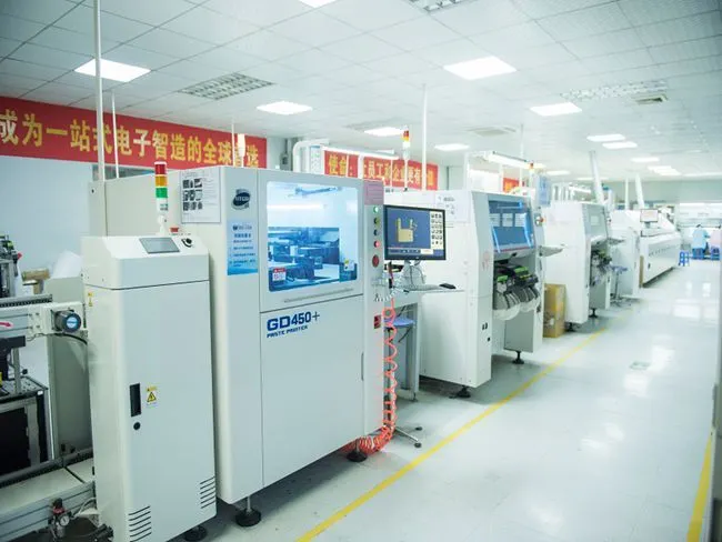
The two processes must be coordinated to avoid assembly defects.
For SMT, solder paste volume, stencil design, component placement, reflow profile, and pad geometry influence joint quality. Large thermal-mass components may require particular attention because they can heat differently from small components on the same board.
For through-hole assembly, hole dimensions, lead fit, solder fill, component seating, and soldering conditions should follow the approved assembly requirements.
Mixed-technology boards may also require a carefully planned process sequence to prevent damage to previously installed components.
7. Solder Joint Reliability and Mechanical Stress
Power supply assemblies can experience repeated temperature changes during startup, operation, shutdown, and environmental cycling. Differences in thermal expansion between components, solder, copper, and PCB materials may create mechanical stress.
Large components can introduce additional stress because of their mass and the forces applied during transport or operation.
To manage these risks, manufacturers should pay attention to:
- Solder joint geometry and workmanship
- Component seating and lead condition
- Thermal profile consistency
- Board support during assembly
- Connector and terminal mounting
- Mechanical reinforcement where specified
- Customer-defined inspection and acceptance criteria
IPC J-STD-001 provides requirements for soldered electronic assemblies, while IPC-A-610 provides visual acceptance criteria. The applicable requirements should be defined in the purchase specification and agreed by the customer and supplier.
8. Inspection and Production Quality Control
Inspection requirements should reflect the component packages, electrical risks, and intended application.
Depending on the assembly design, quality control may include incoming component inspection, solder paste inspection, automated optical inspection, X-ray inspection for selected hidden joints, visual workmanship checks, and electrical or functional tests specified by the customer.
These methods should not be treated as interchangeable. For example, optical inspection can assess visible solder joints and component placement, while X-ray can help examine certain hidden connections. Functional testing evaluates defined operating behaviors but does not automatically replace workmanship inspection.
A clear inspection plan should identify the inspection method, acceptance criteria, sampling or test frequency, records, and responsibility for failure analysis.
For high-power products, system-level verification may also need to address output regulation, efficiency, temperature rise, overload behavior, and protection functions. These tests should be defined by the product manufacturer according to the product specification.
9. What to Include in a High Power Supply PCBA RFQ
A complete RFQ package helps the assembly supplier evaluate manufacturing requirements and identify potential issues before production.
Customers should prepare:
- Gerber files and PCB stackup information
- Complete BOM with approved manufacturer part numbers
- Assembly drawings and centroid data
- Component polarity and orientation information
- Copper thickness and finished board requirements
- Soldering and special handling instructions
- Inspection and acceptance criteria
- Required electrical or functional test specifications
- Prototype and mass-production quantities
- Packaging, labeling, and delivery requirements
The more complete the documentation, the easier it is to assess component availability, process compatibility, and production risks.
High Power Supply PCB Assembly with Ring PCB
Ring PCB provides PCB fabrication, component sourcing, SMT assembly, through-hole assembly, and production quality inspection for a range of electronic manufacturing projects.
Its published PCB process capabilities include heavy-copper construction, with up to 12 oz inner and outer copper for mass production and up to 20 oz for samples. The company also supports multilayer PCB production, with a published maximum of 30 layers for mass production and 70 layers for samples.
For high power supply PCBA projects, customers can submit Gerber files, BOM data, assembly drawings, and specific technical requirements for manufacturing review. Ring PCB can discuss PCB fabrication and assembly feasibility, component sourcing, and production requirements before order confirmation.
To discuss your high power supply PCBA project, contact rfq@ringpcb.com.
References and Further Reading
- IPC — IPC J-STD-001: Requirements for Soldered Electrical and Electronic Assemblies.
- IPC — IPC-A-610: Acceptability of Electronic Assemblies.
- IPC — IPC-2152: Standard for Determining Current-Carrying Capacity in Printed Board Design.
- IPC — IPC-2221: Generic Standard on Printed Board Design.
- Texas Instruments — Power Supply Design and Layout Application Notes.
- Infineon Technologies — Power Semiconductor and PCB Layout Application Guides.