Introduction
The rapid development of AI data centers, cloud computing and high-speed network infrastructure is accelerating demand for advanced optical communication equipment. Optical transceivers, optical networking modules and data center interconnect systems are evolving toward higher transmission rates, greater integration and improved power efficiency.
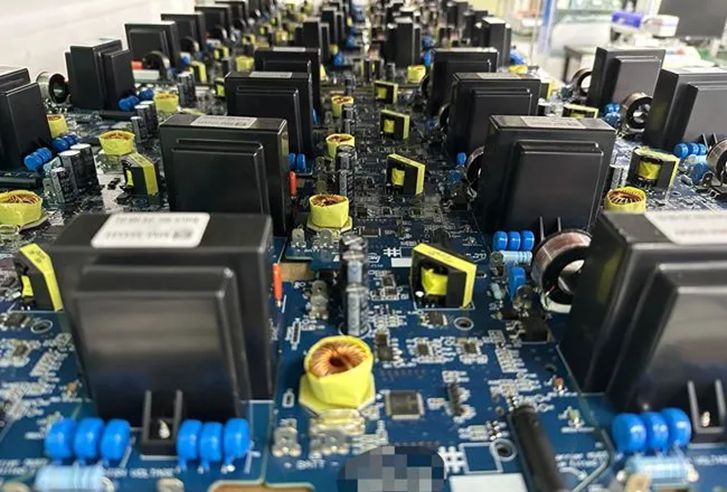
This transition is creating new manufacturing requirements for the electronic circuit boards inside optical communication products. As module designs become more compact and component density increases, Optical Communication PCBA manufacturing must address challenges involving fine-pitch assembly, power distribution, thermal management, electrostatic discharge protection and production consistency.
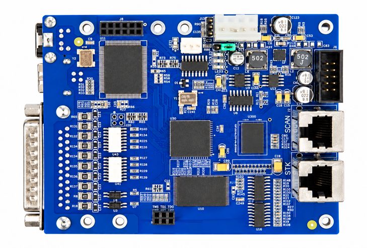
According to TrendForce’s April 2026 forecast, the global AI optical transceiver market is expected to grow from US$16.5 billion in 2025 to US$26 billion in 2026, representing projected year-over-year growth of more than 57%. The report also identifies increasing demand for 800G and 1.6T products as an important market driver.
Meanwhile, the Optical Internetworking Forum (OIF) published its 1600ZR coherent interface agreement in September 2026, establishing an interoperable 1.6T interface for data center interconnect applications.
These developments highlight the importance of reliable electronic manufacturing throughout the optical communication supply chain.
1. Higher-Speed Optical Modules Require More Complex PCBA Manufacturing
Optical communication modules convert electrical signals into optical signals and receive optical signals for conversion back into electrical signals. Their electronic circuitry may include driver ICs, transimpedance amplifiers (TIAs), digital signal processors (DSPs), control circuits, power management components and monitoring devices.
As data rates increase, the electronic circuit boards supporting these functions must accommodate more demanding electrical and mechanical requirements.
For PCBA manufacturers, several challenges become particularly important:
- Higher component density: Compact module structures leave less space for component placement and soldering.
- Fine-pitch packages: Advanced IC packages require accurate solder paste printing and component placement.
- Mixed-signal circuitry: Different circuit functions may have different grounding, power and assembly considerations.
- Thermal sensitivity: High-performance electronic components can generate concentrated heat during operation.
- Mechanical constraints: Board dimensions and connector positions must conform to the customer’s module assembly requirements.
These factors make manufacturing preparation essential. Before production, the PCB Assembly Manufacturer should review the Gerber files, BOM, assembly drawings and relevant technical specifications to identify potential manufacturing concerns.
2. Fine-Pitch SMT Assembly and Component Placement Accuracy
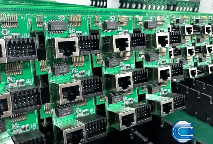
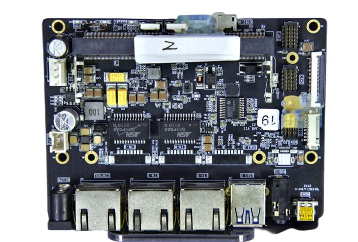
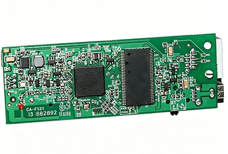
Optical communication boards often contain compact components and high-density electronic packages. As a result, SMT assembly precision becomes an important factor in production quality.
Solder paste printing is one of the first critical stages. Inconsistent paste volume, stencil condition or printing alignment can contribute to solder bridging, insufficient solder or other assembly defects.
Component placement must also be controlled carefully. Fine-pitch ICs, small passive components and connectors may require different placement and inspection considerations.
A controlled SMT process should include:
Solder Paste Printing: Appropriate stencil design, printing parameters and solder paste management help maintain consistent deposition.
Component Placement: Automated pick-and-place equipment supports accurate positioning and orientation according to approved assembly data.
Reflow Soldering: Temperature profiles should be developed according to PCB characteristics, component specifications and soldering requirements.
Post-Reflow Inspection: AOI can identify visible placement and soldering defects, while X-Ray inspection may be appropriate for hidden solder joints beneath BGA packages.
For optical communication PCBA projects, inspection methods should be selected according to package types, assembly complexity and customer quality requirements.
3. Thermal Management and Power Distribution
Higher-speed optical modules often incorporate electronic components with significant power and thermal requirements. DSPs, driver ICs and other active components may generate concentrated heat within a relatively small enclosure.
Although thermal design is primarily determined by the product’s electrical and mechanical architecture, PCBA manufacturing quality also plays an important role.
For example, inconsistent solder joints or poor connections at power-related components can affect electrical performance and reliability. Variations in component placement may also influence the consistency of thermal interfaces where the product assembly depends on specific component positioning.
Manufacturers should therefore pay attention to:
- Consistent solder joint formation.
- Accurate placement of power-related components.
- Appropriate PCB copper and surface finish requirements.
- Manufacturing cleanliness around thermal interface areas.
- Inspection of soldering quality for components exposed to thermal stress.
Thermal management should be considered together with the customer’s PCB specifications and module-level requirements rather than treated as an isolated assembly issue.
4. ESD Protection and Manufacturing Cleanliness
Optical communication products contain sensitive semiconductor devices and high-speed electronic components. Electrostatic discharge (ESD) during handling or assembly can damage sensitive components, sometimes without producing immediately visible symptoms.
For this reason, ESD control should be incorporated into the manufacturing environment.
Typical ESD management measures include:
- Grounded workstations and personnel grounding systems.
- ESD-safe packaging and material handling.
- Appropriate storage conditions for sensitive components.
- Controlled handling procedures during assembly and inspection.
- Personnel training and periodic ESD compliance checks.
Cleanliness is another important consideration. Contamination from dust, solder particles, flux residues or handling can affect electrical connections and subsequent product assembly.
A suitable cleaning process should be determined according to the soldering materials, component sensitivity and customer’s cleanliness requirements. Not every PCBA requires the same cleaning method, and unnecessary cleaning may introduce additional process risks.
For optical modules, the distinction between electronic PCBA manufacturing and optical assembly is also important. Optical alignment, fiber coupling and optical performance verification require specialized equipment and processes. These should be managed by the relevant optical module manufacturer or testing partner unless explicitly included in the agreed manufacturing scope.
5. Inspection and Verification for Optical Communication PCBAs
Inspection requirements should reflect the specific risks of the assembled board.
No single inspection method can identify every potential defect. A combination of inspection and testing methods may be required depending on product complexity.
Automated Optical Inspection (AOI)
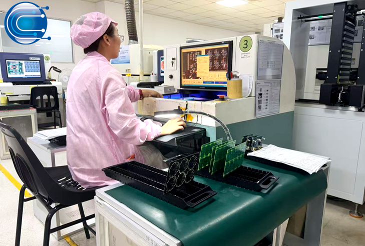
AOI checks visible assembly features such as component presence, orientation, alignment and certain soldering defects. It is useful for detecting common SMT process issues.
X-Ray Inspection
X-Ray inspection can examine hidden solder joints beneath BGA and other suitable package types. It helps identify defects that cannot be reliably assessed through conventional visual inspection.
Electrical Testing
Continuity and other electrical tests can help identify open circuits, short circuits and connectivity problems. The test scope depends on available test access and the customer’s requirements.
Functional Testing
Some optical communication PCBA projects require additional electrical functional verification using customer-defined test procedures. The test plan may cover power-up behavior, control interfaces, communication functions and other specified parameters.
It is important to distinguish PCBA-level electrical testing from complete optical module testing. Optical output power, receiver sensitivity, wavelength accuracy and other optical parameters generally require dedicated optical test equipment and module-level procedures.
6. Managing Product Variants and Manufacturing Consistency
Optical communication equipment manufacturers may develop multiple product versions with different data rates, component configurations, PCB revisions or mechanical interfaces.
This creates additional challenges for PCBA production management.
A manufacturer should maintain clear control over:
- Gerber file revisions.
- BOM versions and approved component manufacturers.
- Assembly drawings and placement data.
- Stencil and process specifications.
- Inspection criteria and test requirements.
- Production batch and material records.
Before repeat production, the approved documentation should be confirmed to prevent outdated files or unauthorized component substitutions from entering the manufacturing process.
For OEMs, this level of manufacturing discipline helps maintain consistency across product variants and recurring orders.
7. What OEMs Should Discuss with a PCB Assembly Manufacturer
When selecting a PCB Assembly Manufacturer for optical communication electronics, buyers should evaluate more than the supplier’s SMT equipment.
A practical manufacturing discussion should cover:
- Whether the supplier can meet the PCB layer count, dimensions and fabrication specifications.
- Whether its SMT equipment supports the required component packages and placement accuracy.
- How solder paste printing and reflow processes are controlled.
- Whether AOI and X-Ray inspection are available where required.
- How sensitive components are handled and protected against ESD.
- How BOM changes and component substitutions are reviewed.
- Whether production records and inspection results can be provided.
OEMs should also clarify the boundary between PCBA manufacturing and complete optical module assembly. This helps ensure that quotation scope, responsibilities and acceptance criteria are clearly defined before production begins.
How Ring PCB Supports Communication PCBA Manufacturing
Ring PCB provides PCB fabrication and PCBA manufacturing services for customers across different electronics sectors, including communication-related applications.
Founded in 2008, Ring PCB operates a 10,000+ sqm self-owned manufacturing facility supported by approximately 500 employees. Its manufacturing capabilities include PCB fabrication up to 62 layers, five automated SMT production lines, component sourcing, through-hole assembly, inspection and testing.
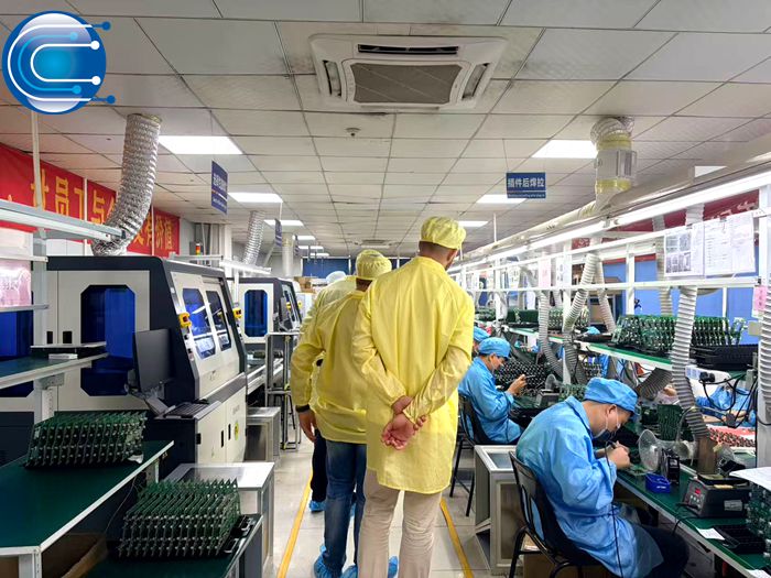
With monthly bare PCB production capacity of approximately 50,000 sqm and the ability to handle around 500 PCBA projects per month, Ring PCB supports different manufacturing volumes and project requirements.
For suitable projects, rapid PCB prototyping can be available in as little as three days, subject to technical specifications and material availability.
Customers can submit Gerber files, BOM data and detailed technical requirements for manufacturing review. Ring PCB communicates with customers to assess production feasibility and confirm the required manufacturing scope before order acceptance.
Conclusion
The development of 800G and 1.6T optical communication products is raising the manufacturing requirements for the electronic circuit boards used in high-speed networking systems.
Fine-pitch SMT assembly, thermal considerations, ESD protection, inspection and revision control all contribute to consistent Optical Communication PCBA manufacturing.
For OEMs, selecting a manufacturing partner with appropriate PCB fabrication and PCBA capabilities can help simplify production coordination and support reliable manufacturing as communication technologies continue to evolve.
If you are looking for PCB fabrication or PCBA manufacturing support for communication electronics, contact Ring PCB to discuss your project requirements.
Email: rfq@ringpcb.com
References and Further Reading
- TrendForce – Global AI Optical Transceiver Market to Reach US$26 Billion in 2026 (April 20, 2026):
- Optical Internetworking Forum (OIF) – 1600ZR Coherent Interface Agreement (September 9, 2026):
- LightCounting – NPO Makes All the Headlines, but the Pluggables Set New Sales Records (September 2026):