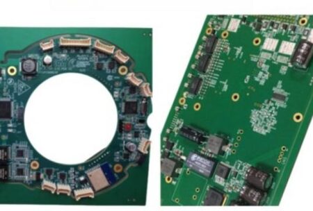
High-power supply systems are becoming more demanding as industrial equipment, data centers, renewable energy systems, and electric mobility applications require greater power density and stable operation.
For these products, PCB performance is influenced by more than the selection of power semiconductors. Copper thickness, layer structure, trace geometry, dielectric materials, thermal paths, component placement, and assembly workmanship all contribute to the final result.
This is why custom PCB manufacturing and assembly are important for high-power supply development. Rather than forcing a complex power circuit into a generic board structure, manufacturers can evaluate the PCB construction and assembly process according to the electrical, thermal, mechanical, and production requirements of the application.
For OEMs, the objective is not simply to create a board with higher current capacity. It is to achieve a manufacturable design that balances performance, reliability, cost, and production scalability.
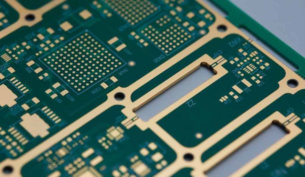
1. Why Standard PCB Structures May Not Be Enough
A conventional PCB structure may be suitable for many control and signal-processing applications. However, high-power supply circuits can impose different requirements.
Power supply boards may carry substantial current, contain components with high thermal dissipation, and combine sensitive control circuits with noisy switching nodes.
A standard PCB construction may not provide the most suitable balance of copper cross-section, thermal distribution, routing space, and mechanical strength.
Custom PCB manufacturing allows the board structure to be evaluated against the actual application.
Important design considerations include:
- Required current and allowable temperature rise
- Copper thickness on individual layers
- Board thickness and layer count
- Trace width, spacing, and routing geometry
- Thermal vias and heat-spreading areas
- Component footprints and terminal structures
- Electrical isolation and voltage requirements
- Manufacturing tolerances and production yield
These parameters should be considered together. Increasing copper thickness, for example, may improve the available conductor cross-section but can also affect etching, plating, fine-line geometry, and overall board construction.
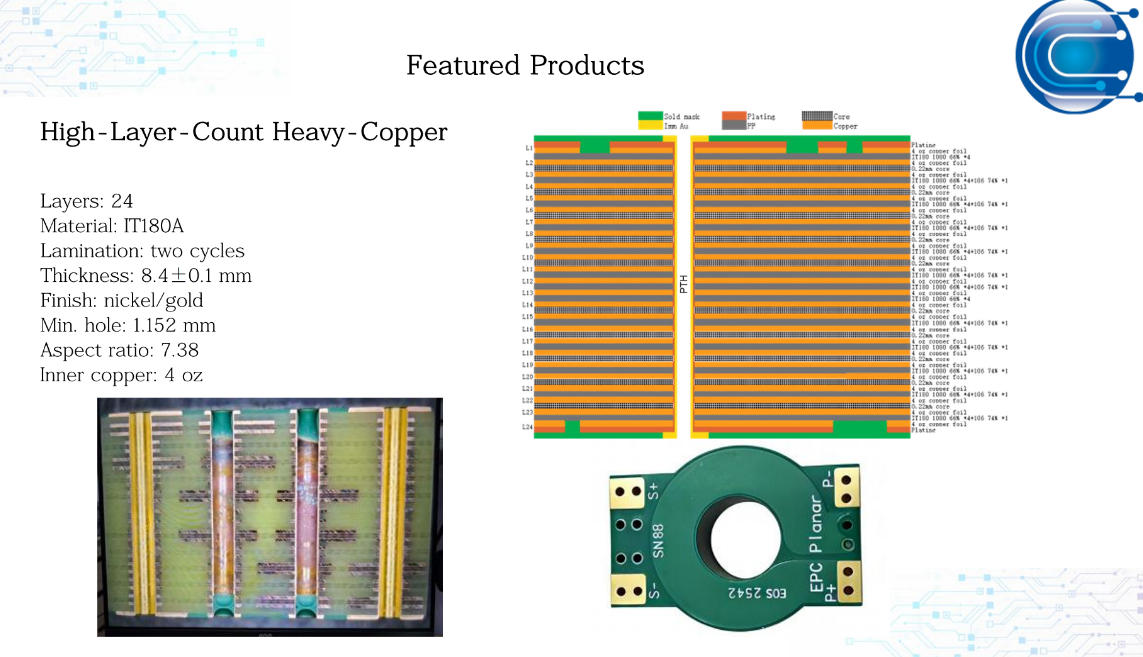
2. Heavy Copper PCB: Supporting High-Current Applications
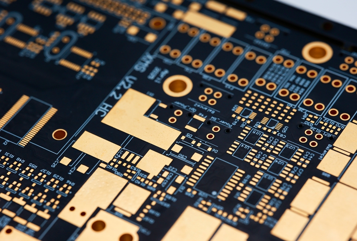
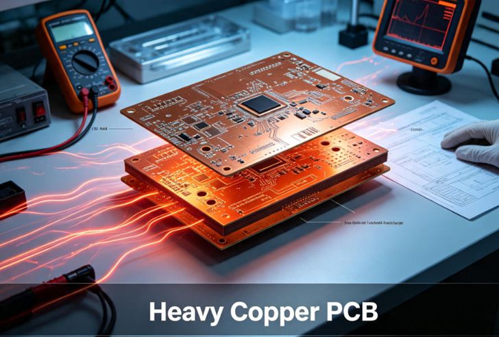
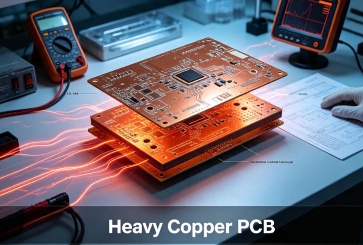
Heavy copper PCB construction is frequently considered for power electronics because it provides a greater copper cross-sectional area than standard copper structures.
For a given conductor geometry, increasing copper thickness can reduce resistance and help manage current-related heating. However, the final current capacity also depends on trace width, conductor length, ambient conditions, allowable temperature rise, and cooling arrangements.
The IPC-2152 standard provides guidance for determining current-carrying capacity in printed board design. Engineers should use the applicable design method and project conditions rather than relying on a simple copper-weight rule of thumb.
Heavy copper also introduces manufacturing challenges.
Etching Control
Thicker copper may require process adjustments to achieve the specified trace width and spacing. The supplier should review the actual copper weight and minimum geometry before production.
Plating Considerations
Copper plating affects finished hole dimensions and conductor structure. The relationship between base copper, plated copper, and finished board requirements should be clearly specified.
Layer-to-Layer Construction
When different copper weights are used across layers, the PCB stackup must be evaluated for manufacturability and dimensional stability.
Fine-Line Limitations
Heavy copper and very fine trace geometry may create competing process demands. A design review can help identify whether the requested copper thickness and routing dimensions are compatible.
Therefore, custom heavy-copper manufacturing should begin with a detailed review of the Gerber data and stackup rather than a general capability assumption.
3. Multilayer Stackup Design for Power and Control Circuits
High-power supply boards often combine power switching, control, sensing, and communication functions.
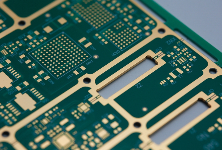
A multilayer PCB can provide more routing space and allow different functions to be distributed across dedicated layers. For example, power distribution, ground reference, control signals, and sensing circuits may require different routing strategies.
However, adding more layers does not automatically improve performance.
The stackup should be developed around the electrical architecture and manufacturing requirements. Relevant considerations include:
Power and Ground Planes
Appropriately designed planes can provide low-impedance return paths and distribute current across the board.
Signal Reference
Control and sensing signals may require stable reference structures to reduce unwanted coupling from switching nodes.
Dielectric Thickness
The spacing between conductive layers affects impedance, capacitance, and the electrical behavior of the board.
Copper Balance
Copper distribution should be considered during stackup planning to support fabrication stability and reduce potential warpage.
Thermal Distribution
Internal copper layers may help spread heat, but the effectiveness depends on how heat is transferred to the board surface, heat sink, or enclosure.
For this reason, the stackup should be reviewed by both the design team and the PCB manufacturing partner before production.
4. Thermal Management Through PCB Construction
Thermal management is a major concern in high-power supply systems.
Power semiconductors, rectifiers, inductors, transformers, and high-current conductors can all contribute to local heat generation. If the thermal path is inadequate, hot spots may develop around components or copper connections.
Custom PCB manufacturing can support thermal management through several construction features.
Thermal Via Arrays
Plated thermal vias can transfer heat between layers and toward a copper plane or heat-spreading structure.
Copper Areas
Larger copper regions may distribute heat across the PCB, depending on the layout and the thermal interface to the rest of the system.
Component Pad Design
Pad geometry and soldering requirements should be reviewed for power devices with exposed thermal pads or large terminals.
Board Material and Thickness
The laminate and board construction should meet the project’s electrical, mechanical, and thermal requirements.
Nevertheless, PCB construction is only one part of the thermal solution. Heat sinks, airflow, cooling plates, enclosure design, and system-level thermal validation remain important.
5. Managing Switching Noise and Signal Integrity
High-power converters often contain fast-switching semiconductor devices. Their operation can create rapid voltage and current transitions, making parasitic inductance, return paths, and electromagnetic coupling important design considerations.
A custom PCB layout should pay attention to the physical size of switching current loops, the placement of decoupling capacitors, and the separation between noisy power nodes and sensitive control circuits.
Gate-driver routing, current-sensing connections, and feedback paths may also require careful layout.
A manufacturing partner cannot replace the circuit designer’s responsibility for power-stage topology or electromagnetic compatibility. However, it should be able to manufacture the approved copper geometry, layer structure, and dimensional requirements consistently.
For this reason, customers should provide complete fabrication data and clarify any critical impedance, isolation, or tolerance requirements before ordering.
6. Assembly Design: Making High-Power Boards Manufacturable
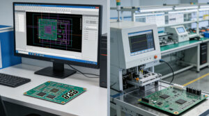
PCB fabrication and component assembly should be reviewed as connected stages.
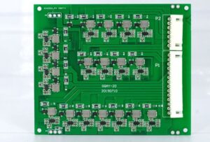
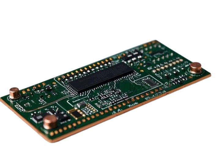
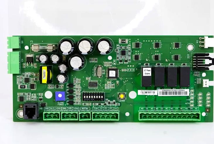
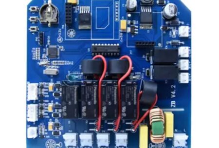
A high-power supply board may combine small SMT control components with large transformers, inductors, capacitors, connectors, and power devices.
These components may require different assembly methods and thermal conditions.
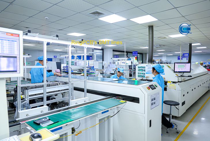
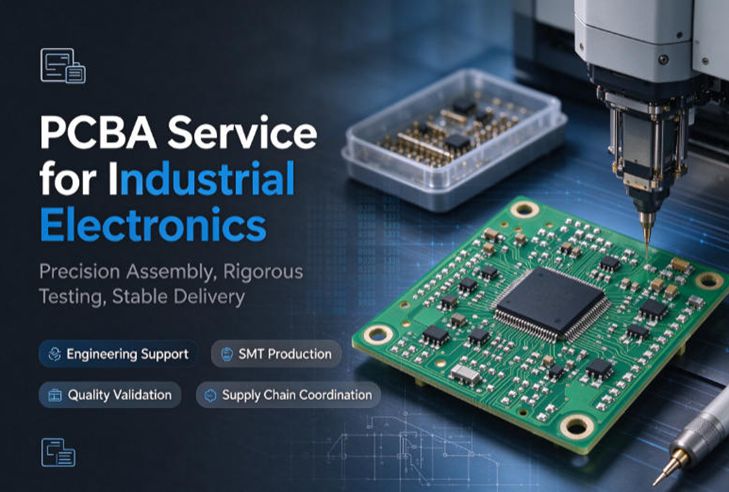
SMT assembly supports automated placement of many control and power components. Through-hole assembly may be appropriate for larger connectors, terminals, and components requiring mechanical support.
Several details should be considered before assembly:
- Package and footprint compatibility
- Component polarity and orientation
- Solder paste and stencil requirements
- Reflow profile limitations
- Through-hole dimensions and lead fit
- Board support during soldering
- Thermal mass of large components
- Inspection access and acceptance criteria
Large components can absorb heat differently from small SMT devices, so assembly conditions should be evaluated for the actual board and component mix.
7. Manufacturing Feasibility Review: Reducing Cost and Production Risk
A technically attractive PCB design may still be difficult or expensive to manufacture.
For example, a combination of very heavy copper, tight line spacing, high layer count, and thick finished board requirements may create process constraints.
A manufacturing feasibility review can identify these issues before the order enters production.
Useful review topics include:
Minimum Line and Space: Confirm that trace dimensions are compatible with the specified copper thickness.
Hole and Via Requirements: Review minimum hole diameter, aspect ratio, annular ring, and plating requirements.
Board Thickness: Check whether the required thickness is compatible with the layer structure and drilling process.
Impedance Requirements: Confirm the target impedance, tolerance, and relevant stackup details where controlled impedance is required.
Panel Size and Production Format: Evaluate panel dimensions and manufacturing utilization.
Assembly Compatibility: Review component packages, board dimensions, and assembly requirements.
These checks can help avoid unnecessary design changes, quotation delays, and production rework.
8. From Prototype to Repeatable Production
A custom PCB should be evaluated not only for prototype feasibility but also for repeat production.
Prototype builds can help verify the fabrication structure, assembly documentation, component compatibility, and initial workmanship. First Article Inspection may be used to compare an initial build with the agreed requirements.
Before mass production, the customer and manufacturer should confirm the PCB revision, BOM, approved component sources, assembly instructions, and inspection criteria.
Engineering changes should also be controlled. A change in copper weight, dielectric thickness, component footprint, or alternative component may affect manufacturing feasibility and should be reviewed before implementation.
A stable production process depends on consistent documentation and clear communication between the customer and manufacturer.
9. Choosing a Custom PCB Manufacturing and Assembly Partner
When evaluating a supplier for high-power supply boards, OEMs should consider both fabrication and assembly capabilities.
Important questions include:
- What layer count and copper weight can the supplier support for production and samples?
- Can it manufacture the required board thickness and panel dimensions?
- Does it support the specified line, space, hole, and impedance tolerances?
- Can it provide both SMT and through-hole assembly?
- Can it source components according to an approved BOM?
- How are manufacturing questions and proposed substitutions communicated?
- What inspection methods are available for the project?
- Can the supplier review prototype and mass-production requirements separately?
A supplier should be selected according to demonstrated process capabilities and the specific requirements of the project, not only a broad claim of supporting high-power PCBs.
Custom PCB Manufacturing and Assembly with Ring PCB
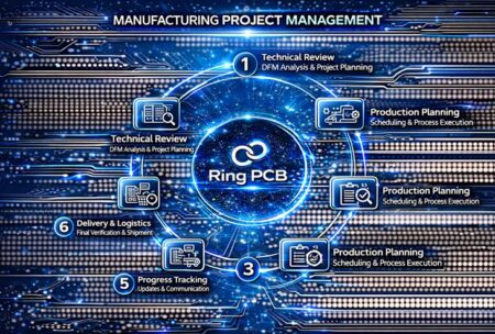
Ring PCB provides PCB fabrication, component sourcing, SMT assembly, through-hole assembly, and production quality inspection. Its published process capabilities include up to 12 oz inner and outer copper for mass production and up to 20 oz for samples. The company lists multilayer production capability of up to 30 layers for mass production and 70 layers for samples.
Its process range also includes controlled-impedance requirements, backdrilling, blind and buried vias, and HDI structures, subject to the specified process limits and project review.
For high-power supply projects, customers can submit Gerber files, stackup information, BOM data, assembly drawings, and technical requirements for manufacturing evaluation. Ring PCB can discuss the feasibility of the required PCB construction, component sourcing, and assembly process before confirming order acceptance.
To discuss a custom high-power PCB or PCBA project, contact rfq@ringpcb.com.
References and Further Reading
- International Energy Agency — Energy and AI (2025).
- IPC — IPC-2152: Standard for Determining Current-Carrying Capacity in Printed Board Design.
- IPC — IPC-2221: Generic Standard on Printed Board Design.
- IPC — IPC J-STD-001: Requirements for Soldered Electrical and Electronic Assemblies.
- IPC — IPC-A-610: Acceptability of Electronic Assemblies.
- Texas Instruments — Power Supply Design and PCB Layout Application Resources.