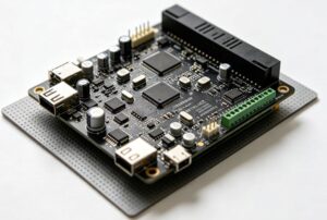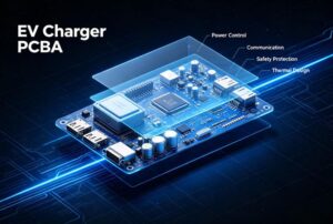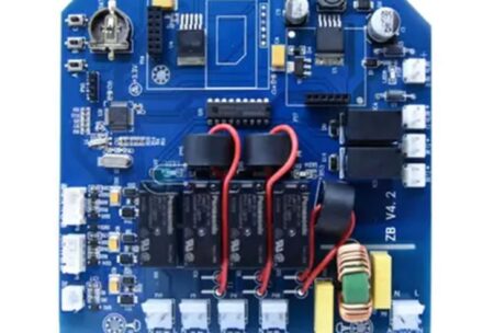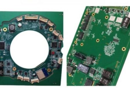
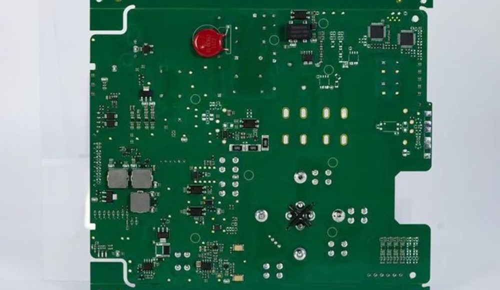
Against the backdrop of booming global EV charging infrastructure deployment, charger OEMs are under mounting pressure to launch new products faster while keeping bill-of-materials costs under control. 2026 industry research reveals that nearly 58% of EV charger new product programs experience 6–8 week launch delays and 15–25% budget overruns, most of which stem from misalignment between PCB design and actual manufacturing capabilities. Many engineering teams prioritize electrical performance and feature richness in early development, but overlook process feasibility, material availability and production yield — issues that only surface when designs move to volume manufacturing.
For smart EV charger PCBA, which integrates high-voltage power circuits, signal control modules and communication interfaces, even minor design flaws can trigger costly re-spins, low assembly yield and unstable field performance. Adopting a Design for Manufacturability (DFM) -first approach, with manufacturing engineers involved from the earliest design phase, resolves these issues at the source. This article examines the hidden costs of design-manufacturing disconnect in charger PCBA development, explains how proactive DFM optimization drives down total cost and shortens launch cycles, and outlines best practices for implementing this model.
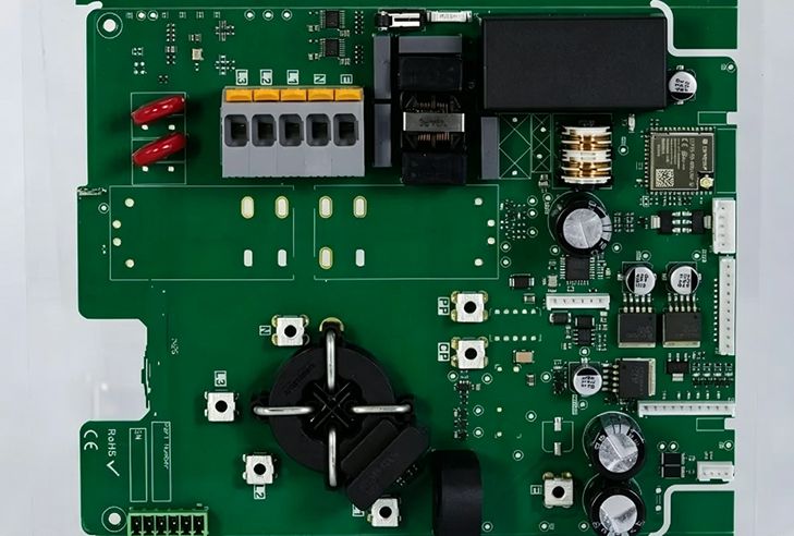
1. The Hidden Cost of Poor DFM in EV Charger PCBA Development
At first glance, skipping formal DFM review seems to save time in the design stage. In reality, it transfers risks and costs to later production phases, where fixes are exponentially more expensive.
First, unreasonable trace and via design for high-power paths directly reduces production yield. For 30kW+ DC charger PCBA, insufficient copper width, poorly planned thermal vias or misaligned pad dimensions can cause local overheating, solder voids and delamination during reflow. These issues rarely appear in lab prototype testing, but emerge as systematic defects in automated volume production, dragging first-pass yield down by 20–30%.
Second, component selection without supply chain visibility creates procurement risks. Engineers often specify preferred semiconductors based on datasheet performance alone, without verifying long-term availability, lead times or second-source options. With power semiconductors and SiC devices still facing allocation pressure in 2026, designing with single-sourced components can halt production overnight when stock runs out.
Third, non-standardized form factors and test point placement increase assembly and testing costs. Designs that cannot be panelized efficiently waste substrate material, while missing or inaccessible test points force manual inspection, raising per-unit labor costs and slowing throughput.
2. Four Core Value Streams of DFM-First PCBA Manufacturing
When manufacturing expertise is embedded early in the design cycle, charger OEMs gain measurable benefits across cost, speed, quality and supply resilience.
2.1 Reduced Production Cost Through Yield and Material Optimization
Experienced PCBA manufacturers review stack-up configuration, copper weight distribution and panelization layout before finalizing the design. For heavy copper charger boards, they recommend optimized trace geometries and via stitching patterns that improve thermal performance while maintaining etchability. Better panelization alone can reduce PCB material waste by 12–18%, directly lowering unit cost. They also suggest form-fit-function component alternatives with stable supply and lower pricing, trimming BOM cost by 8–15% without sacrificing performance.
2.2 Shorter Time-to-Volume by Eliminating Design Re-Spins
Every design iteration after prototype testing adds weeks to the launch schedule. Proactive DFM review catches manufacturability issues before the first board is ever fabricated, reducing prototype re-spins by an average of 40–60%. For charger OEMs racing to capture market windows, this can mean launching 2–3 months earlier than competitors using a traditional design-then-outsource model.
2.3 Improved Long-Term Reliability and Lower Warranty Exposure
DFM optimization is not only about production efficiency — it also improves field reliability. Engineers identify high-stress areas such as AC-DC isolation boundaries, connector mounting points and thermal hotspots, and recommend design reinforcements such as teardrop pads, copper thieving and reinforced creepage distances. These changes reduce field failure rates over the 10+ year service life, cutting warranty and service costs substantially.
2.4 Built-In Compliance Readiness
Global markets require EV chargers to meet IEC 61851, CE, UL and local safety standards. DFM reviews include compliance checks for creepage, clearance, insulation spacing and trace temperature rise. Catching compliance violations during design avoids expensive rework and certification retesting later in the program.
3. Executing a Smooth Ramp-Up: From Design Review to Volume Production
Realizing these benefits requires more than a one-time document check. It requires close collaboration between the OEM’s engineering team and the PCBA manufacturer throughout the development journey.
Ring PCB integrates DFM review as a standard step in our EV charger PCBA turnkey service, with dedicated power electronics engineers assigned to every customer project. Our team reviews Gerber files, BOM lists and assembly drawings at the earliest design stage, providing detailed optimization recommendations covering PCB stack-up, thermal layout, component sourcing security, panelization efficiency and test point placement. We do not just flag problems — we propose specific, actionable redesign suggestions that balance performance, cost and manufacturability.
Beyond initial DFM, we support customers through prototype validation, pilot runs and full volume ramp-up with consistent process standards across all phases. Component engineers pre-validate alternative parts and secure volume allocation before ramp-up, preventing supply disruptions. Our in-house testing lab performs thermal cycling, insulation withstand and EMC pre-compliance testing during the pilot phase, so issues are resolved before mass production begins. This end-to-end DFM-driven approach typically reduces our customers’ total launch timeline by 25–35% compared to conventional separated design and manufacturing workflows.
4. Key Selection Criteria for DFM-Capable Charger PCBA Partners
Not all PCBA suppliers deliver meaningful DFM value. When evaluating partners, charger OEMs should verify three factors: first, whether the supplier has dedicated power electronics engineering staff with direct EV charger experience, not just general PCB technicians; second, whether DFM review is included as a standard service rather than a paid add-on; and third, whether the supplier can support the full journey from prototype through mass production, so DFM insights actually carry over to volume manufacturing.
Conclusion
In the fast-evolving EV charging market, speed-to-market and cost control directly determine competitive success. Rushing through design and skipping DFM review creates far greater costs and delays downstream. A DFM-first approach to EV charger PCBA manufacturing reduces material waste, improves production yield, shortens launch timelines and improves long-term reliability, delivering value that far outweighs the upfront review effort. For charger OEMs, partnering with a manufacturer that brings manufacturing expertise into the early design stage is no longer a nice-to-have — it is a strategic necessity.
If you are developing a new EV charger product and want to optimize your design for manufacturability, cost and reliability, send your design files and project timeline to rfq@ringpcb.com. Ring PCB‘s power electronics engineering team will provide a comprehensive DFM assessment and launch roadmap within 24 working hours.