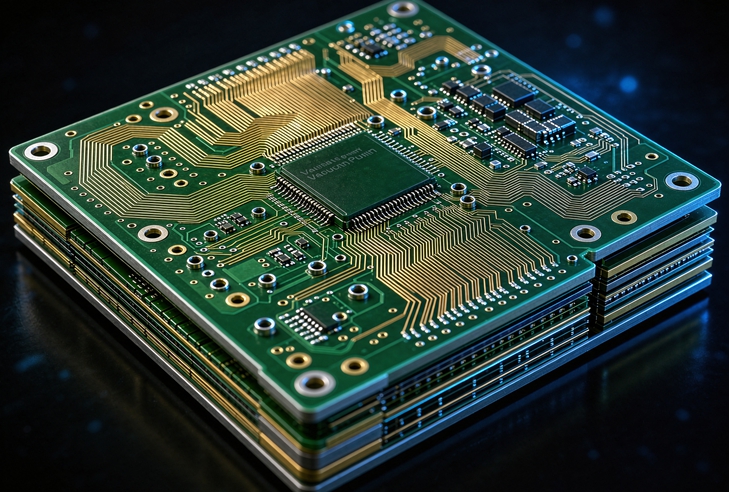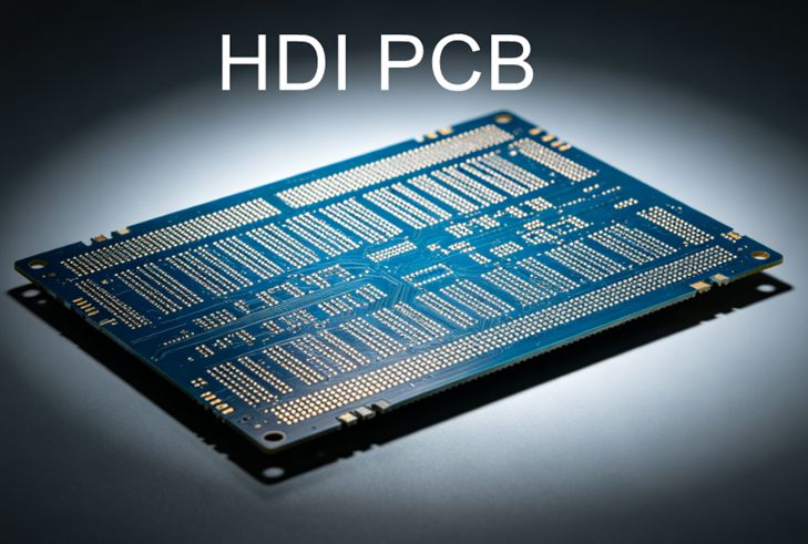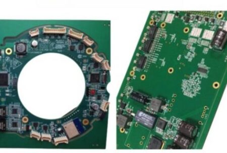
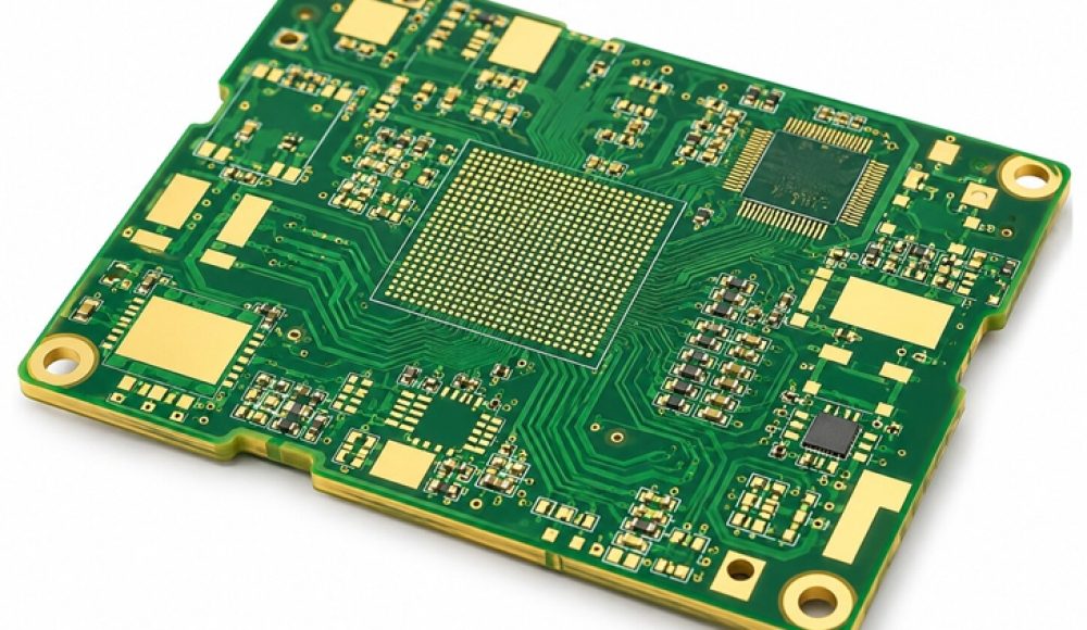
High-density interconnect (HDI) PCBs have become an important solution for electronic products that require more functionality in less space. As components become smaller and package pin counts increase, conventional through-hole structures may consume too much routing area. HDI technology addresses this challenge through finer conductor patterns, laser-drilled microvias, blind vias, buried vias, and sequential lamination.
For OEMs developing communication equipment, industrial electronics, medical devices, and compact computing systems, selecting an HDI PCB manufacturer involves more than checking minimum trace width or the number of build-up layers. The board’s interconnection structure, material system, manufacturing sequence, and microvia reliability must work together.
This guide explains the main HDI PCB manufacturing considerations and the questions buyers should address before releasing a design for production.
1. What Makes an HDI PCB Different?
An HDI PCB uses high-density interconnection structures to increase routing capacity within a limited board area. Its construction may combine conventional multilayer core layers with additional build-up layers.
Unlike a traditional multilayer PCB that relies mainly on mechanically drilled plated through-holes, an HDI board can use several types of interlayer connections:
- Blind vias: Connect an outer layer to one or more selected inner layers without passing through the entire board.
- Buried vias: Connect internal layers and remain invisible from the external board surfaces.
- Microvias: Small-diameter vias, commonly formed by laser drilling, that connect adjacent or selected build-up layers.
- Stacked microvias: Microvias positioned vertically above one another to connect multiple build-up layers.
- Staggered microvias: Microvias offset from one another, providing connections between layers without direct vertical alignment.
These structures help free routing space, particularly around fine-pitch components such as BGAs and chip-scale packages.
2. Choosing the Right HDI Stackup
The stackup determines how copper layers, dielectric materials, and interconnection structures are arranged. A suitable structure should meet routing requirements without adding unnecessary manufacturing complexity.
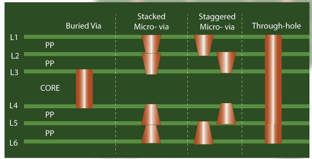
Common HDI constructions include 1+N+1, 2+N+2, and more complex sequential build-up structures. The letter N represents the core layers, while the numbers indicate the build-up layers on each side.
For example, a 2+N+2 construction provides two build-up layers on each side of the core. This can support more routing channels and component escape options than a simpler structure.
However, more build-up layers do not automatically produce a better board. Additional lamination cycles, microvia interfaces, and alignment requirements can increase fabrication complexity. Therefore, engineers should first identify the actual routing bottleneck and then select the least complex structure that meets the electrical and mechanical requirements.
For projects involving stacked or staggered microvias, the manufacturer should review the via arrangement, target-pad dimensions, dielectric thickness, and copper-plating requirements before the stackup is finalized.
3. Microvia Diameter and Laser Drilling
Laser drilling is widely used to form small blind microvias in HDI build-up layers. Compared with conventional mechanical drilling, laser processing allows smaller via diameters and more precise connections between adjacent layers.
A typical microvia diameter may be around 0.1 mm, although the appropriate size depends on the dielectric thickness, target pad, copper structure, and manufacturing process.
The via aspect ratio is another important consideration. A microvia that is too deep relative to its diameter may be more difficult to metallize consistently. For this reason, via diameter and dielectric thickness should be evaluated together rather than specified independently.
Before releasing the design, OEM engineers should confirm:
- Laser via diameter and depth
- Target-pad and capture-pad dimensions
- Via-to-copper clearance
- Whether vias are stacked or staggered
- Filling and capping requirements, if applicable
- The manufacturer’s achievable aspect ratio
These checks help prevent a design from depending on dimensions that cannot be reproduced reliably in production.
4. Microvia Reliability: The Importance of Interfaces
Although microvias improve routing density, their small dimensions make manufacturing quality particularly important. A microvia is not simply a hole connecting two copper layers. Its reliability also depends on the interface between the via copper and the target copper.
Potential issues include incomplete copper filling, voids, poor interface bonding, insufficient plating, and defects caused by unsuitable drilling or surface preparation.
Stacked microvias require particular attention because multiple interconnections are aligned vertically. Their interfaces experience manufacturing and thermal stresses during fabrication and subsequent product use. Staggered structures may reduce some alignment and interface demands, although the best choice depends on the design.
For demanding applications, buyers should ask how the supplier controls laser drilling, desmear, metallization, copper filling, and sequential lamination. They should also establish suitable inspection and qualification requirements based on the product’s operating environment.
IPC’s HDI-related standards, including IPC-2226 and IPC-6016, provide relevant design and performance references. The applicable revision and acceptance requirements should be agreed upon by the customer and manufacturer.
5. Via-in-Pad and Plated Over Filled Vias
When fine-pitch components leave little room for conventional fan-out routing, via-in-pad can provide a compact interconnection option. A via is placed directly within a component solder pad, allowing signals to move into internal layers without using additional surface routing space.
However, an open via in a solder pad can create soldering problems. Solder may flow into the hole during reflow, reducing the solder volume available for the component joint.
Plating over filled vias (POFV) addresses this issue through a controlled filling and plating process. The via is filled with resin or copper paste and then plated over to create a flatter, more continuous surface.
This structure can help preserve the soldering area and reduce solder wicking into the via. It is particularly relevant to dense BGA layouts and other applications where component pitch and available pad area are limited.
The filling material, surface flatness, plating quality, and finished pad dimensions should be included in the manufacturing discussion.
6. Materials and Thermal Considerations
HDI boards often use thin dielectric layers and compact copper structures. Material selection therefore affects electrical performance, mechanical stability, and manufacturing compatibility.
The material system should be evaluated according to dielectric properties, thermal performance, moisture behavior, dimensional stability, and compatibility with the selected lamination process.
For example, a compact HDI board used in a high-speed communication product may require a different material strategy from a low-frequency industrial controller. The design should not select a laminate solely because it has a familiar brand name or a favorable data-sheet value.
Engineers should also consider copper distribution. Large differences in copper density between layers can contribute to uneven lamination behavior and dimensional variation. Balanced copper distribution and a carefully reviewed stackup can help improve manufacturing consistency.
7. What to Check When Selecting an HDI PCB Manufacturer
Before choosing a supplier, buyers should review more than its advertised minimum feature size.
Important questions include:
- What HDI structures can be produced in mass production?
- What laser via diameters and aspect ratios are supported?
- Can the supplier manufacture stacked and staggered microvias?
- What filling and capping processes are available?
- How are lamination alignment and microvia interfaces controlled?
- Which material systems can be processed?
- What inspection and qualification evidence can be provided?
It is also important to distinguish prototype capability from repeatable mass-production capability. A supplier may accept a highly advanced sample construction, but the same construction may require additional review before it can be released for stable production.
HDI PCB Manufacturing with Ring PCB
Ring PCB provides multilayer and HDI PCB fabrication for projects with demanding interconnection and routing requirements. Its published process capability lists 2+N+2 HDI for mass production and ELIC for sample capability. The process table also specifies laser via diameters of 0.10–0.20 mm for mass production and 0.075–0.5 mm for samples.
In addition, Ring PCB supports blind and buried vias, laser drilling, POFV, and other specialized PCB processes. Its manufacturing capability includes up to 30 layers for mass production and up to 70 layers for samples. Actual feasibility depends on the complete construction, materials, dimensions, and project requirements.
For an HDI PCB quotation, customers can submit Gerber files, stackup information, BOM data where assembly is required, and specific technical requirements for manufacturing review. Ring PCB also provides component sourcing, SMT and through-hole assembly, and production quality inspection.
To discuss your next HDI PCB project, contact rfq@ringpcb.com.
References and Further Reading
- IPC — IPC-2226, Sectional Design Standard for High Density Interconnect (HDI) Printed Boards.
- IPC — IPC-6016, Qualification and Performance Specification for High Density Interconnect (HDI) Structures.
- IPC — Technical papers on microvia design and reliability.
- Altium Resources — High-Density Interconnects: A Design and Manufacturing Guidebook.
- European Cooperation for Space Standardization — ECSS-Q-ST-70-12C, Microvia Technology.