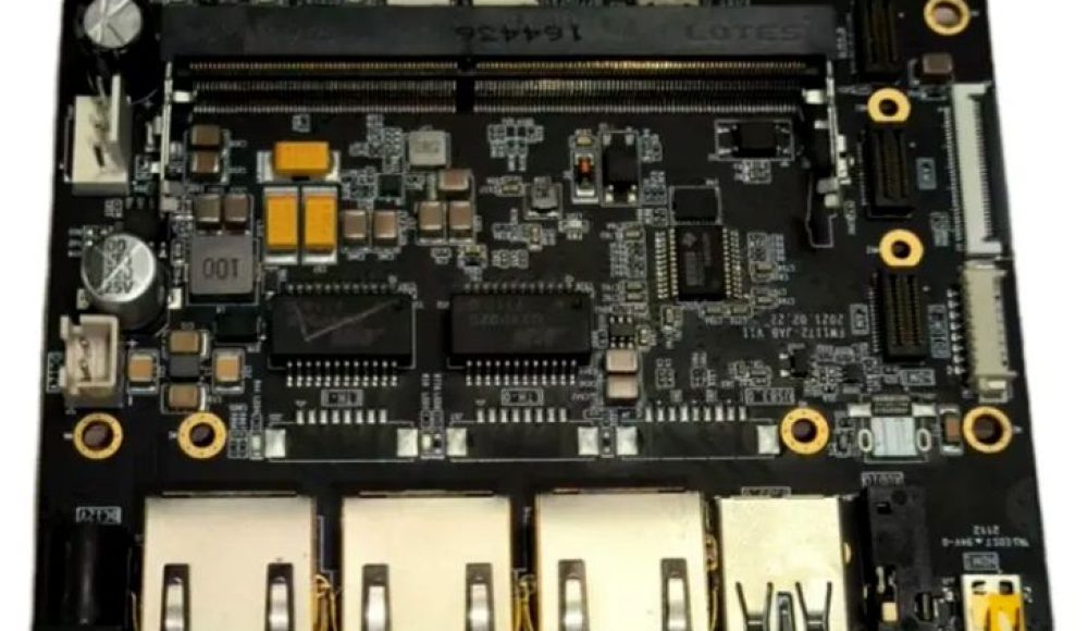
Communication equipment manufacturers face a challenge that cannot be solved by selecting faster processors alone: the PCB assembly must preserve signal quality throughout the entire electronic system.
Ethernet switches, wireless gateways, optical network controllers, and high-speed communication modules increasingly combine dense components, high-speed interfaces, and complex power distribution networks. A board may pass basic electrical checks while still experiencing intermittent data errors, excessive insertion loss, or unstable performance.
According to Ericsson’s June 2026 Mobility Report, mobile network data traffic increased 22% year over year in the first quarter of 2026. This growth does not directly measure PCB demand, but it illustrates the increasing performance expectations placed on communication infrastructure.
For OEMs, successful High-Speed PCB Assembly requires close cooperation between electrical engineering, PCB fabrication, component sourcing, and PCBA manufacturing.
Why Signal Integrity Matters Beyond PCB Design
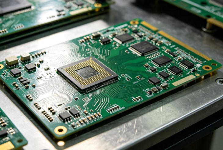
Signal integrity describes how accurately electrical signals travel between transmitting and receiving components.
At higher data rates, transmission-line effects become increasingly important. Impedance discontinuities, reflections, crosstalk, and excessive losses can reduce the available signal margin.
These problems are often associated with PCB layout, but manufacturing variation can also influence performance.
Changes in dielectric thickness, copper geometry, via structures, or material properties may affect the finished transmission lines.
Furthermore, assembly-related issues such as connector misalignment, solder defects, or incorrect component substitutions can introduce additional problems.
Therefore, a PCBA Manufacturer should understand which electrical parameters are critical before beginning production.
Controlled Impedance Starts With the Stackup
Controlled impedance is a fundamental requirement for many high-speed communication boards.
The electrical characteristics of a transmission line depend on trace width, copper thickness, dielectric thickness, dielectric constant, and reference-plane geometry.
For example, differential interfaces may require a specified differential impedance, while RF signal paths often use single-ended transmission lines.
The exact target must come from the design specification rather than a generic manufacturing assumption.
During DFM review, the PCB Manufacturer should verify the proposed stackup against available materials and fabrication tolerances.
If adjustments are necessary, the manufacturer should obtain engineering approval before modifying critical trace geometry.
For suitable projects, impedance coupons and measurement reports can provide additional manufacturing verification.
Material Loss Becomes More Important at Higher Frequencies
Not every communication PCB requires an expensive high-frequency laminate.
Many Ethernet and networking applications can use appropriate FR-4 materials, depending on the channel length, data rate, and loss budget.
However, higher-frequency RF circuits or demanding high-speed links may benefit from lower-loss materials.
Important properties include dielectric constant (Dk), dissipation factor (Df), thermal stability, and manufacturing compatibility.
Material selection should also consider availability and production consistency.
Substituting a different laminate without evaluating its electrical characteristics may change signal loss or impedance behavior.
Consequently, material approval should be part of the controlled manufacturing documentation.
Vias, Connectors, and Transitions Need Attention
Signal quality can deteriorate at transitions between transmission-line structures.
Examples include plated through-hole vias, layer changes, connectors, component pads, and changes in reference planes.
At sufficiently high frequencies, unused via stubs can contribute to reflections and insertion loss.
Backdrilling or alternative via structures may be appropriate for selected designs, although they increase manufacturing complexity and should be justified by engineering analysis.
Similarly, connector footprints and launch geometry can affect channel performance.
A manufacturing review should identify these critical features rather than focusing only on minimum trace width and spacing.
Assembly Quality Affects High-Speed Performance
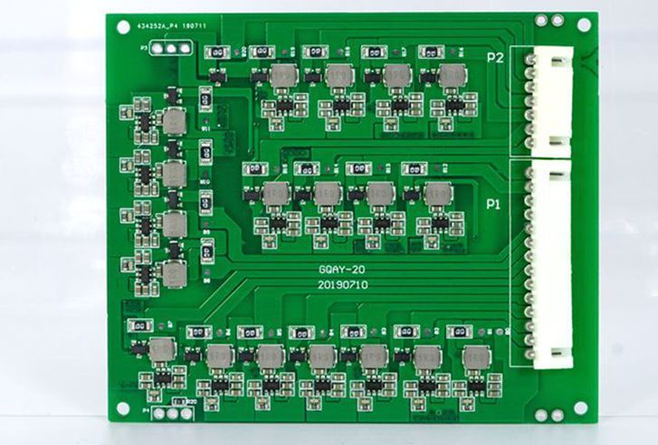
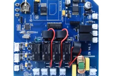
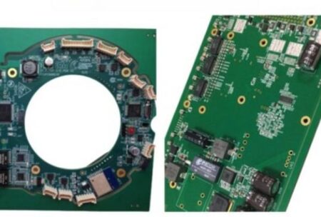
Modern communication PCBAs often use BGAs, QFNs, fine-pitch connectors, and small passive components.
Reliable assembly requires accurate solder paste printing, component placement, and reflow control.
A solder defect beneath a BGA may create intermittent connections that are difficult to identify through basic visual inspection.
X-ray inspection can help evaluate hidden solder joints, while AOI detects visible placement and soldering defects.
However, neither method directly measures the signal integrity of a completed high-speed channel.
This distinction matters because manufacturing inspection and electrical performance validation serve different purposes.
OEMs should define both requirements in the production plan.
Power Integrity and EMI Cannot Be Ignored
High-speed processors and communication ICs require stable power supplies.
Power-distribution noise can affect timing margins, signal quality, and system stability.
Meanwhile, poorly controlled return-current paths may increase electromagnetic interference.
Although these issues originate primarily in circuit and PCB design, manufacturing must preserve the approved stackup, component values, and assembly configuration.
Decoupling capacitor substitutions, for example, should be reviewed for relevant electrical characteristics and package compatibility.
A full-turnkey assembly service can coordinate these requirements between sourcing and engineering teams before purchasing decisions are finalized.
How Should High-Speed Communication PCBAs Be Tested?
Testing should match the product’s intended function and critical interfaces.
Basic checks may include power sequencing, current consumption, firmware programming, and interface communication.
More demanding applications may require bit error rate testing, eye-diagram analysis, signal-loss measurements, or protocol-specific validation.
RF assemblies may require different specialized instruments and acceptance criteria.
Importantly, a PCBA Manufacturer should not claim that AOI or ordinary continuity testing proves high-speed signal performance.
Specialized electrical tests should be defined by the OEM, with responsibilities and fixtures agreed before production.
Preventing Prototype-to-Production Performance Changes
A successful prototype does not guarantee identical results during volume production.
Material substitutions, stackup changes, different fabrication tolerances, or revised components can alter electrical behavior.
Therefore, pilot builds should validate the intended manufacturing configuration.
Critical materials, PCB revisions, approved components, and test requirements should be documented.
When changes become necessary, their potential impact on signal integrity should be assessed before implementation.
This approach supports repeatability without requiring every board to undergo laboratory-level characterization.
Ring PCB’s Role in High-Speed Communication Manufacturing
Reliable high-speed communication electronics require manufacturing discipline across multiple processes.
Ring PCB supports communication PCBA projects with multilayer and high-frequency PCB fabrication, controlled-impedance manufacturing capabilities, component sourcing, SMT and THT assembly, engineering review, inspection, and full-turnkey assembly services.
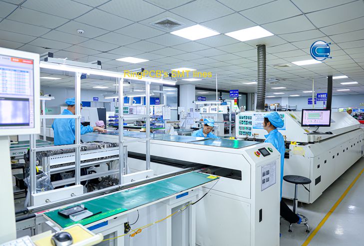
Its integrated PCB and PCBA manufacturing workflow helps customers coordinate fabrication requirements with downstream assembly needs.
For communication boards involving high-speed interfaces, dense components, or specialized materials, early review of the stackup and manufacturing files can help identify potential production risks.
Send your Gerber or ODB++ files, BOM, stackup specifications, assembly drawings, and testing requirements to rfq@ringpcb.com.
References
- Ericsson. Ericsson Mobility Report: 5G Subscriptions Top Three Billion as Uplink Gains Momentum. June 16, 2026.
- Ring PCB. Custom 10 Layer PCB Manufacturing Solution. Manufacturing and controlled-impedance capability information.
- Ring PCB. FR-4 Communication PCBA. Communication PCB fabrication and assembly applications.