Design for manufacturability (DFM) is the most ignored yet impactful step in multilayer PCBs manufacturing. Many hardware engineers finish schematic and layout with perfect simulation results, only to face low yield, extended lead times or unexpected cost increases after sending files to factories. The root cause is simple: design work often overlooks real manufacturing limits. Working closely with a one-stop PCB & PCBA manufacturer at the early design phase helps avoid such costly mistakes.
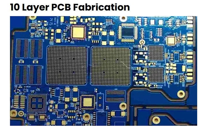
Common DFM Mistakes for Multilayer PCB Projects
The first common mistake is unreasonable stack-up planning. For high-layer PCBs, asymmetric stack-up causes severe board warpage during lamination and reflow soldering, damaging assembly quality. Many designers only focus on signal routing and ignore copper balance across layers. Second, insufficient consideration of via aspect ratio. Deep vias in thick multilayer boards increase plating difficulty. If the hole diameter is too small compared with board thickness, incomplete copper plating on via walls will occur. Third, ignoring trace width and spacing rules. Fine lines on inner layers are vulnerable to open or short circuits during etching. Fourth, mismatched pad sizes for SMT components, which will create soldering issues in later PCBA assembly.
These errors are easy to avoid with early DFM review. A skilled manufacturer can flag these risks before mass production starts, rather than discovering defects after the first batch is finished.
How a One-Stop PCB & PCBA Manufacturer Improves DFM Outcomes
When multilayer PCBs manufacturing and PCBA assembly sit under one supplier, DFM review covers both bare board production and soldering requirements. Separated suppliers usually only check PCB fabrication rules and neglect SMT risks.
The one-stop team will examine your Gerber and BOM from two angles: PCB fabrication feasibility and assembly compatibility. For example, they will evaluate whether high-speed stack-up maintains stable impedance, check thermal pad design for BGA components, and adjust hole sizes to fit plating capacity. This joint review reduces revision rounds and cuts overall project cycle. Especially for high-layer boards over 32 layers, this integrated review can greatly raise the first-pass yield.
Industry Trends Require Closer Designer-Manufacturer Collaboration
In 2026, AI servers and high-speed communication hardware push multilayer PCB specs tighter. Controlled impedance, low-loss material and higher layer counts become mainstream requirements. In this environment, passive “send files and wait for boards” procurement no longer works. Successful projects require continuous technical communication between design teams and manufacturing partners.
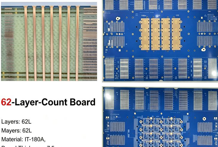
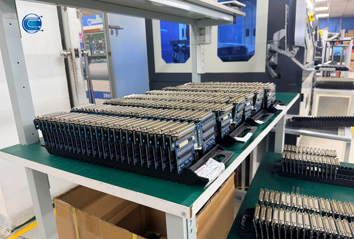
Ring PCB, as a professional one-stop PCB & PCBA manufacturer with deep multilayer PCBs manufacturing capability, offers free DFM assessment for incoming projects. We support high multilayer PCBs up to 62 layers. Our monthly capacity reaches 50,000 ㎡ bare PCBs, and we can manage up to 500 PCBA projects monthly to serve diverse projects from prototype to medium batch. Our engineering team reviews layer stack-up, via structure, impedance requirements and assembly risks together. Our full-range production equipment guarantees stable quality for complex multilayer boards and subsequent PCBA assembly.

If you plan a multilayer PCB design and want a professional DFM check and quotation before production, send your design documents to rfq@ringpcb.com.