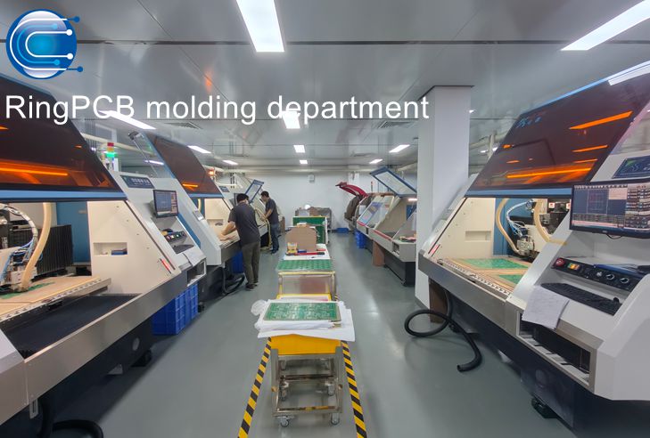
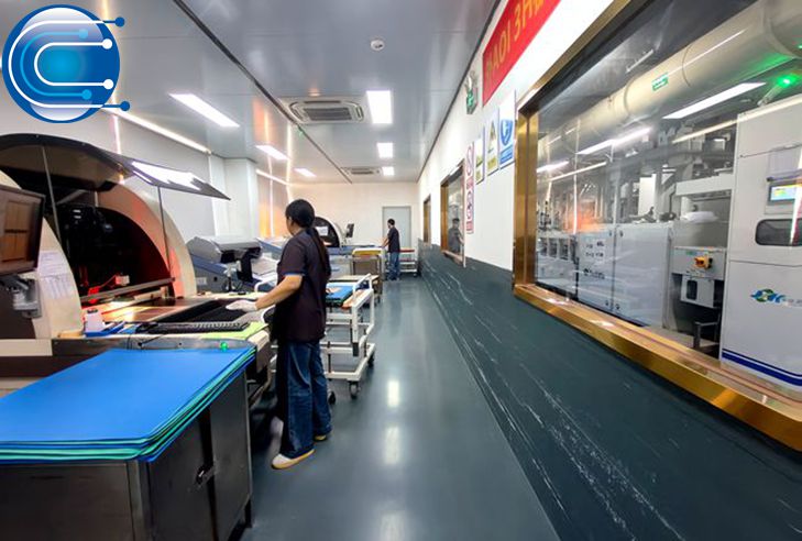
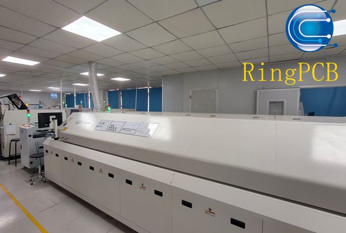
Ring PCB heavy Copper Based PCB Manufacturer, Fast Prototype & Full Turnkey PCB PCBA One-Stop Solution
Product Description
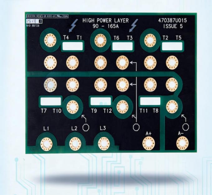
What Is a 2-Layer Heavy Copper PCB?
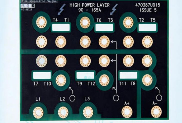
A 2-layer heavy copper PCB is a specialized printed circuit board designed to carry extremely high current while maintaining electrical stability and thermal reliability. Compared with standard copper PCBs, heavy copper PCB manufacturing uses significantly thicker copper layers—typically ranging from 3 oz up to 20 oz or more—to support high-current transmission and enhanced heat dissipation.
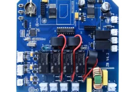
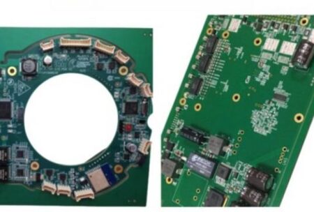
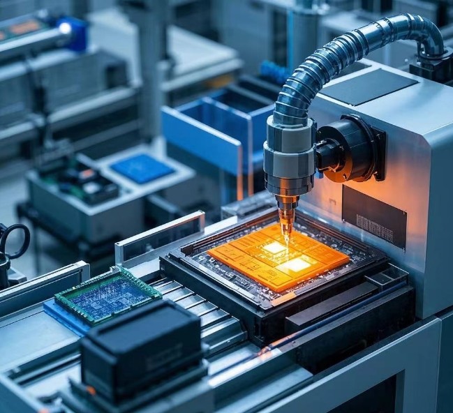
The heavy copper PCB shown in the image is a customized solution manufactured for a customer’s high-power application, presented for reference to demonstrate Ring PCB’s heavy copper PCB manufacturing capabilities.
This type of PCB is widely used in power electronics, industrial control systems, power distribution units, motor drives, energy storage systems, and high-current equipment.
Key Features and Advantages of Copper Based PCB
1. Excellent Heat Dissipation
Copper has outstanding thermal conductivity, allowing fast heat transfer from critical components. This significantly improves product stability and lifespan.
2. High Mechanical Strength
A Copper based PCB provides better mechanical rigidity and durability, suitable for harsh environments and industrial-grade applications.
3. High Current Carrying Capacity
Thanks to thick copper layers and a solid metal core, Copper based PCB designs can handle high current loads with minimal power loss.
4. Superior Reliability
Reduced thermal stress and improved heat distribution help minimize failure rates, especially in high-power LED, automotive, and power electronics.
5. Customizable Structure
Ring PCB supports full customization of Copper based PCB stack-ups, copper thickness, surface finish, and overall design to meet specific industry needs.
Typical Technical Parameters of Copper Based PCB (For Reference Only)
| Parameter | Specification Range |
|---|---|
| Base Material | Copper |
| Copper Thickness | 1 oz – 10 oz |
| Board Thickness | 0.8 mm – 3.2 mm |
| Thermal Conductivity | ≥ 380 W/m·K |
| Dielectric Thickness | 75 μm – 150 μm |
| Surface Finish | HASL, ENIG, OSP, Immersion Silver |
| Solder Mask Color | Green, White, Black, Blue |
| Application Temperature | -40℃ to +150℃ |
Note:
The above parameters are for reference only. Final specifications and designs depend on your project requirements.
Please contact our professional customer service team for customized solutions: info@ringpcb.com
FAQ – 2-Layer Heavy Copper PCB Manufacturing
Q1: What applications are best suited for 2-layer heavy copper PCBs?
They are ideal for power supplies, industrial power control systems, motor drives, power distribution modules, and energy management equipment.
Q2: How thick can the copper be for heavy copper PCBs?
Ring PCB supports customized copper thicknesses, typically ranging from 3 oz up to 20 oz or more, depending on application requirements.
Q3: Can Ring PCB provide PCB assembly for heavy copper PCBs?
Yes. We offer one-stop PCB & PCBA services, including SMT, through-hole assembly, testing, and full turnkey solutions.
Q4: Do you provide PCB design services?
Ring PCB does not offer direct PCB design services, but we provide DFM support to help optimize customer designs for manufacturability and reliability.
Q5: What is the lead time for heavy copper PCB manufacturing?
We support 3-day rapid prototyping and 7-day mass production, depending on design complexity and order quantity.
If you are interested in our Heavy copper PCB circuit boards, please provide your customized needs, we will complete the sample production within 3 working days, and complete mass production and delivery within 15 working days.
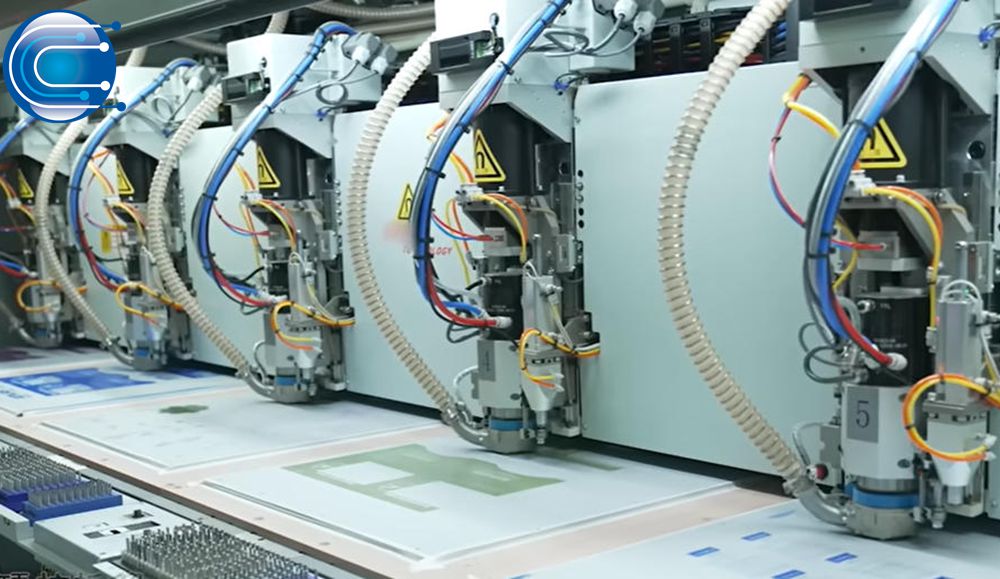
One-Stop Service for PCB and PCBA Solutions!
Ring PCB’s Key Advantages
-
Advanced Engineering for Precision PCB Manufacturing
-
High-Density Stack-Up: 2-48 layer boards, ideal for 5G, industrial control, medical devices, and automotive electronics.
-
Smart Manufacturing: Self-owned facilities with LDI laser exposure, vacuum lamination, and flying probe testers, ensuring compliance with IPC-6012 Class 3 standards.
-
-
Integrated PCBA Services | One-Stop Turnkey Solutions
-
Full Assembly Support: PCB fabrication, component sourcing, SMT assembly, and functional testing, all under one roof.
-
DFM/DFA Optimization: Our expert engineering team optimizes designs to reduce risks and BOM costs, enhancing efficiency.
-
Rigorous Quality Control: X-ray inspection, AOI testing, and 100% functional validation ensure zero-defect delivery.
-
-
Self-Owned Factory with Full Supply Chain Control
-
Vertical Integration: We manage raw material procurement, production, and testing in-house, ensuring maximum control over the production process.
-
Triple Quality Assurance: AOI, impedance testing, and thermal cycling with a defect rate of <0.2% (industry average: <1%).
-
Global Certifications: ISO9001, IATF16949, and RoHS compliance to meet international standards.
-
Why Choose Ring PCB?
-
18Years of Excellence in PCB and PCBA manufacturing, offering high-quality, reliable products for critical applications.
-
Self-Owned Factories ensure full control over the production process, allowing us to meet strict deadlines and guarantee consistent quality.
-
End-to-End Technical Support: From design and prototyping to mass production and final assembly, we provide comprehensive support at every stage.
-
Fast Turnaround: Prototype production within 3 days and mass production within 7 days to keep your projects on schedule.
-
Global Reach: Serving customers in over 50 countries with ongoing industrial partnerships.
Contact Us
📧 Email: rfq@ringpcb.com