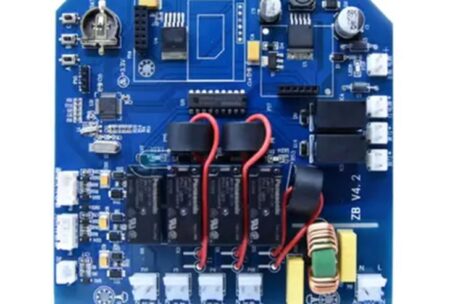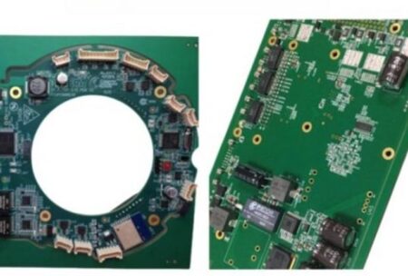
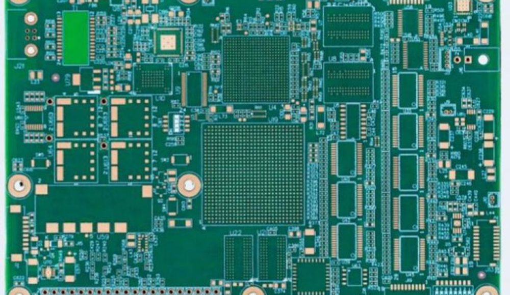
Power electronics are the backbone of renewable energy inverters, industrial motor drives, EV charging systems and high-current power conversion hardware. As global equipment designers pursue higher power density, standard thin-copper circuit boards struggle to handle continuous heavy current, thermal buildup and long-cycle operation. In this context, custom heavy copper PCBA manufacturing has evolved from an optional upgrade to a fundamental requirement for stable power electronic systems. This article explores market trends, core technical challenges, and why tailored heavy copper assembly directly impacts equipment uptime and total operating costs for B2B OEMs.
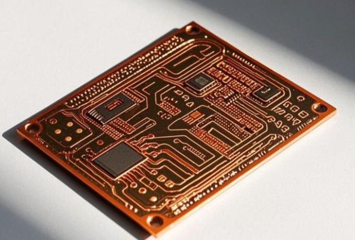
1. Market Growth Driven by Rising Demand for High-Current Hardware
First of all, booming investment in new energy and industrial automation fuels sustained expansion of the heavy copper PCB sector. According to independent market research, the global heavy copper PCB market reached USD 2.495 billion in 2025, maintaining a year-on-year growth rate above 10%, far exceeding the average growth rate of the overall PCB industry.
Furthermore, nearly 68% of heavy copper board demand originates from power electronics fields: electric vehicle power modules, photovoltaic inverters, industrial variable-frequency drives and energy storage equipment. Conventional 1oz or 2oz PCBs create obvious bottlenecks for these devices. Excessive I²R power loss, overheating traces and voltage drop become common failure risks under continuous heavy loads. As a result, more hardware developers choose custom heavy copper PCBA solutions to match their unique power parameters instead of generic circuit boards.
2. Core Pain Points That Standard PCBs Cannot Resolve in Power Electronics
To understand the value of heavy copper manufacturing, we first examine the inherent limitations of ordinary circuit boards for high-power applications. Above all, thin copper traces suffer severe thermal stress when carrying large currents. Heat generated by resistance cannot dissipate quickly, raising local board temperatures. Industry data confirms that every 10°C temperature rise can shorten the service life of power semiconductors by roughly half. In addition, serious voltage drop on thin traces reduces power conversion efficiency, raising long-term energy consumption for end users.
Besides thermal risks, vibration and thermal cycling bring hidden reliability threats. Standard copper layers are prone to solder joint fatigue and trace delamination under repeated temperature swings, which is unacceptable for industrial and automotive power equipment designed for 5–10 years of service. For these reasons, power electronics OEMs must adopt heavy copper PCBs with copper thickness ranging from 3oz up to 10oz or thicker.
3. Key Advantages of Custom Heavy Copper PCBA for Power Electronic Projects
Custom heavy copper PCBA brings three irreplaceable strengths for power electronics development. Initially, thicker copper layers deliver higher current-carrying capacity and lower resistive loss. Customized copper thickness, track width and layout can be precisely matched to your peak and continuous current demands, effectively reducing overheating and energy waste.
Secondly, heavy copper acts as an enhanced thermal conduction path. Copper boasts far higher thermal conductivity than FR-4 substrate. Properly designed heavy copper layouts spread heat away from IGBTs, MOSFETs and other heat-generating power components, lowering reliance on bulky external heat sinks and supporting compact equipment design.
Last but not least, customized manufacturing allows engineers to optimize stack-up, material selection and mechanical structure. Unlike off-the-shelf boards, tailor-made heavy copper PCBA can meet special requirements such as wide-temperature operation, vibration resistance and strict impedance control, fully adapting to harsh factory and outdoor operating environments.
4. Manufacturing Expertise Determines the Consistency of Heavy Copper PCBA
Heavy copper production carries unique technical barriers compared with standard PCB fabrication. Precise etching control, stable multi-layer lamination and controlled surface treatment are mandatory to avoid trace distortion, insufficient copper thickness and inner layer defects. Poor manufacturing control will directly cause unstable performance during continuous high-load operation.
Choosing an experienced EMS partner is critical to avoid costly prototype revisions and mass production failures. Ring PCB specializes in custom heavy copper PCB and turnkey PCBA manufacturing for power electronics customers. With 18 years of production experience, our factory supports heavy copper boards ranging from 3oz to 12oz, widely used in inverters, industrial power modules and EV charging equipment.
We provide full-service solutions including PCB fabrication, authorized component sourcing, precision SMT/THT assembly and multi-stage quality testing. Our engineering team offers complimentary DFM reviews early in the design phase, optimizing trace layout, thermal paths and copper thickness schemes to balance reliability and manufacturing cost. All products comply with ISO9001, IATF16949 and UL standards, with strict AOI, X-ray and functional load testing before shipment. Whether you need small-batch prototype verification or stable long-term mass production, we can accommodate power electronics projects of different scales.
Conclusion
To sum up, custom heavy copper PCBA manufacturing is not merely a material upgrade, but a necessary technical foundation for reliable modern power electronics. Faced with the trend of higher power density and stricter reliability standards, OEMs that adopt tailored heavy copper assembly gain clear advantages in equipment efficiency, lifespan and market competitiveness.
If you are developing power conversion hardware and require custom heavy copper PCBA solutions, send your Gerber files, BOM and technical specifications to rfq@ringpcb.com. Our engineering team will provide professional technical suggestions and a competitive quotation within 24 working hours.