A multilayer PCB can look complete in a CAD system while still containing manufacturing risks that affect cost, electrical performance, and production yield. For OEM engineers developing industrial controllers, communication equipment, medical electronics, or embedded computing systems, these risks often become visible only after the first fabrication batch.
The challenge becomes greater as layer counts increase. Inner-layer alignment, dielectric thickness, copper distribution, drilling accuracy, and lamination behavior must all remain within defined limits.
Therefore, successful Multilayer PCB Manufacturing requires more than selecting a layer count. It demands early coordination between electrical requirements and fabrication capabilities.
A manufacturing-focused stackup review helps engineers reduce avoidable revisions before PCB fabrication and assembly begin.
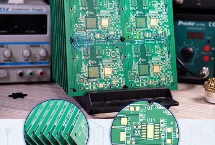
Why Multilayer PCB Stackup Planning Matters
A PCB stackup defines the arrangement of copper layers, dielectric materials, and reference planes.
Its structure influences signal integrity, power distribution, electromagnetic compatibility, board thickness, and mechanical stability.
For example, a six-layer industrial controller may use dedicated ground and power planes to support processors, communication interfaces, and mixed-signal circuits.
A higher-layer-count networking board may require additional reference planes and controlled-impedance routing layers.
However, adding layers does not automatically improve performance.
The stackup must match the electrical design, available materials, manufacturing tolerances, and cost objectives.
Early stackup planning allows the engineering team to identify these constraints before routing is finalized.
Balance Signal Layers and Reference Planes
High-speed signals need appropriate reference paths.
Poor reference-plane continuity can increase return-current discontinuities, electromagnetic emissions, and signal integrity problems.
Consequently, multilayer designs should consider the relationship between signal layers, ground planes, and power distribution.
Critical routing layers may benefit from adjacent solid reference planes.
Meanwhile, sensitive analog circuits and switching power sections may require additional layout consideration.
The exact arrangement depends on the product’s electrical requirements.
A PCB Manufacturer should review the proposed stackup for fabrication feasibility without making unauthorized changes to the intended electrical structure.
Understand Dielectric Thickness and Impedance Control
Controlled impedance depends on more than the nominal trace width.
Dielectric thickness, copper thickness, dielectric constant, and transmission-line geometry all influence the finished result.
During fabrication, manufacturing adjustments may be necessary to compensate for process characteristics.
However, changes to critical impedance features should be reviewed against the customer’s electrical requirements.
For applications requiring verification, impedance test coupons can help assess selected structures.
Engineers should specify impedance targets, tolerances, and relevant layers clearly.
This information allows the manufacturer to determine whether the proposed stackup can be produced consistently.
Layer Registration and Lamination Challenges
Multilayer PCB fabrication requires accurate alignment of inner-layer circuitry before lamination.
Misregistration can reduce annular ring margins, affect drilled-hole alignment, and create electrical reliability risks.
Lamination also introduces material movement and dimensional changes.
These effects must be considered when defining drill targets, layer alignment allowances, and feature tolerances.
For high-layer-count boards, the cumulative impact of multiple manufacturing stages becomes especially important.
A qualified manufacturer should use appropriate process controls and inspection methods to manage these variables.
OEMs should avoid specifying unnecessarily restrictive tolerances that increase cost without improving product performance.
Copper Balance and Board Warpage
Copper distribution affects more than current-carrying capacity.
Uneven copper coverage across layers may influence lamination behavior, mechanical stability, and board warpage.
Warpage can also create downstream problems during SMT assembly.
For example, excessive deformation may affect solder paste contact, component placement, or BGA soldering.
Therefore, copper balance should be reviewed during both PCB fabrication planning and assembly preparation.
Where appropriate, engineers may adjust copper distribution or panelization while preserving electrical requirements.
This illustrates why fabrication and assembly considerations should not be treated independently.
Select Via Structures Based on Actual Requirements
Through-hole vias remain suitable for many multilayer PCB applications.
However, dense layouts may require blind vias, buried vias, or microvias.
These structures can improve routing flexibility but also introduce additional manufacturing steps and reliability considerations.
For example, sequential lamination and complex drilling requirements may increase production cost.
Via-in-pad structures may require filling and planarization before assembly.
The correct choice depends on component density, routing requirements, signal performance, and production volume.
A DFM review should determine whether advanced via structures are necessary or whether a simpler approach can meet the design requirements.
Consider PCB Surface Finish and Assembly Compatibility
The surface finish protects exposed copper and supports component soldering.
Common options include HASL, ENIG, immersion silver, and other application-dependent finishes.
Each has different considerations involving planarity, storage, cost, and process compatibility.
Fine-pitch components may benefit from a relatively planar surface.
However, the appropriate finish should be selected according to the assembly process and product requirements.
The manufacturer should also review solder mask clearances, pad geometry, and component footprint compatibility.
These details become important when a multilayer PCB moves directly into SMT and through-hole assembly.
Use DFM Review Before Releasing Manufacturing Files
An effective DFM review examines whether the approved PCB design can be manufactured consistently.
Typical topics include minimum trace and spacing, drilling structures, annular rings, copper-to-edge clearance, stackup, impedance requirements, and panelization.
For projects using One-Stop PCB Assembly Service, the review should also consider component spacing, solder mask design, assembly access, and inspection requirements.
This broader evaluation helps identify conflicts between bare-board fabrication and component assembly.
Importantly, DFM recommendations should be communicated to the OEM for approval.
Manufacturing review supports the customer’s design process; it does not replace electrical or PCB design responsibility.
Verify Quality Against Defined Requirements
Multilayer PCB quality should be assessed using appropriate fabrication specifications and customer requirements.
IPC-6012F provides an industry reference for rigid printed board qualification and performance.
Depending on the product, verification may include electrical testing, dimensional inspection, impedance measurement, and microsection analysis.
The inspection plan should reflect the board’s complexity and intended application.
For assembled boards, separate workmanship and functional testing requirements also apply.
This distinction prevents confusion between bare-board quality and finished PCBA performance.
Multilayer PCB Manufacturing With Ring PCB
Successful multilayer PCB projects begin with a manufacturable stackup and continue through controlled fabrication and assembly.
Ring PCB provides multilayer PCB fabrication, engineering DFM review, component sourcing, SMT and THT assembly, inspection, and One-Stop PCB Assembly Service.

Its integrated manufacturing workflow helps OEMs coordinate PCB fabrication requirements with downstream assembly processes.
For multilayer boards involving controlled impedance, dense components, or specialized materials, early technical review can help identify potential manufacturing constraints before production.
Send your Gerber files, stackup information, BOM, assembly drawings, quantities, and technical specifications to rfq@ringpcb.com for a manufacturing quotation.
References
- IPC. Recently Released IPC Standards and Documents. Includes IPC-6012F, Qualification and Performance Specification for Rigid Printed Boards.
- IPC. IPC Releases “J” Revisions to Two Leading Standards for Electronics Assembly. April 8, 2024.
- Ring PCB. Multilayer PCB Manufacturing: Key Risks Solved by Full-Turnkey PCB & PCBA Partnerships. September 11, 2026.