When your circuit needs more routing space without increasing the board footprint, a Multilayer PCB can give you the layer density, signal control, and design flexibility you need. However, complex boards also create challenges in layer alignment, impedance control, fine-line fabrication, and assembly quality. Ring PCB provides custom multilayer PCB manufacturing and one-stop PCBA services, helping you move from prototype design to volume production with controlled processes and documented quality standards.
What Is a Multilayer PCB?
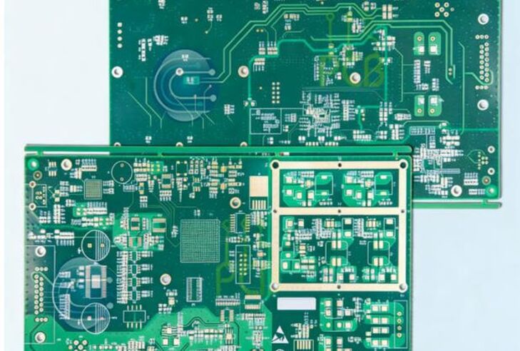
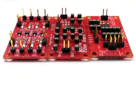
A Multilayer PCB contains three or more conductive copper layers laminated with insulating materials. By distributing signal, power, and ground networks across different layers, you can accommodate more circuits within a compact board structure.
For applications with demanding routing requirements, multilayer construction can support:
- Higher circuit density
- More organized signal and power distribution
- Better control of high-speed signals
- Improved space utilization
- Greater flexibility for complex electronic designs
Ring PCB manufactures multilayer boards for industrial control, medical electronics, telecommunications, automotive electronics, and high-speed systems.
Custom Multilayer PCB Manufacturing Capabilities
Your PCB requirements may vary significantly depending on circuit density, operating environment, material selection, and production volume. Ring PCB supports customized manufacturing from prototypes through mass production.
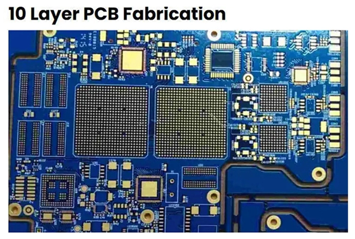
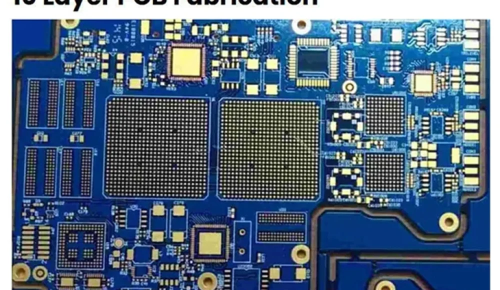
The featured product is a 10-layer PCB with a minimum line width and spacing of 3mil/3mil. It uses an impedance-controlled design and is intended for applications where signal integrity and compact routing are important.
Key manufacturing specifications include:
- Layer count: 4–16 layers for this product specification
- Board thickness: 0.8–3.2 mm
- Copper thickness: 1–6 oz
- Minimum line width/spacing: 3mil/3mil
- Materials: FR-4, High-Tg FR-4, Rogers
- Surface finishes: ENIG, HASL, OSP, Immersion Silver
- Operating temperature: -40°C to 85°C
- Inspection: AOI and X-ray inspection
- Customization: Layer count, materials, copper thickness and finish
At the company level, Ring PCB can fabricate high-multilayer PCBs up to 62 layers, giving you options when your project goes beyond conventional multilayer designs.
Multilayer PCB vs. Other PCB Structures
Choosing the right PCB structure depends on your routing complexity, product size, signal requirements, and budget.
| PCB Type | Circuit Density | Typical Advantage | Suitable Applications |
|---|---|---|---|
| Single-Sided PCB | Low | Simple and economical | Basic electronics |
| Double-Sided PCB | Medium | More routing space | Industrial controls |
| Multilayer PCB | High | Complex routing and signal management | Medical, telecom, automotive |
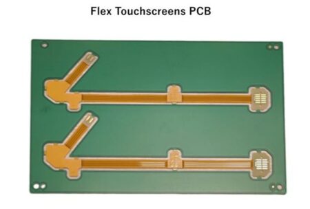
| Flexible PCB | High | Bending and space optimization | Wearable and compact devices |
| Rigid-Flex PCB | High | Combines rigid and flexible structures | Advanced electronics |
If your design requires multiple power, ground, and signal layers within a limited footprint, a custom multilayer PCB can provide a practical manufacturing approach.
How Ring PCB Manufactures a Multilayer PCB
A controlled manufacturing workflow helps reduce defects and maintain consistent electrical performance. You can follow these typical steps when developing your board with Ring PCB:
- Submit your PCB files and specifications
Provide Gerber files, layer information, BOM data, stack-up requirements, and other relevant design documents. - Engineering review and DFM analysis
Ring PCB reviews the design for manufacturability, including line spacing, layer alignment, drilling, impedance, and material requirements. - Material preparation and inner-layer fabrication
The production team processes copper layers according to the approved stack-up and circuit design. - Lamination and drilling
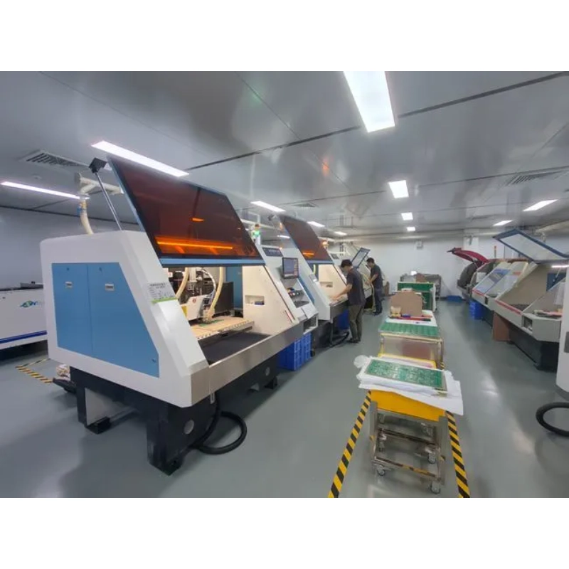
Multiple layers are aligned and laminated before CNC drilling creates the required holes and vias. - Circuit formation and surface finishing
The board undergoes imaging, etching, solder mask application, surface finishing, and other required processes. - Inspection and electrical testing
AOI, X-ray inspection, and other quality-control procedures help identify manufacturing issues before delivery. - PCB assembly and final testing
If you need a complete product solution, Ring PCB can continue with SMT, THT assembly, component sourcing, testing, and inspection.
One-Stop Multilayer PCB Assembly and PCBA
PCB fabrication is only one part of your electronics manufacturing project. If you need a complete supply chain, Ring PCB provides full-turnkey PCB assembly, including component procurement, BOM management, SMT assembly, through-hole assembly, functional testing, and quality inspection.
This integrated model can simplify supplier coordination and help you manage prototype and production requirements through one manufacturing partner.
Ring PCB operates approximately 10,000 square meters of manufacturing facilities with around 500 employees. Its production capacity reaches approximately 50,000 m² of bare PCBs per month and up to 500 PCBA projects per month.
For development projects, Ring PCB also supports 3-day PCB prototyping, while established production programs can move into larger-scale manufacturing.
Quality Standards and Manufacturing Experience
When you source a multilayer board for regulated or demanding applications, manufacturing credentials matter. Ring PCB operates according to internationally recognized quality and environmental management standards.
Relevant certifications and compliance credentials include:
- ISO9001 quality management
- ISO14001 environmental management
- ISO13485 medical device quality management
- IATF16949 automotive quality management
- UL certification
- RoHS and REACH-related compliance support
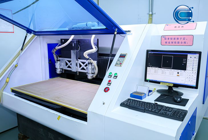
Since 2008, Ring PCB has supplied tens of thousands of PCB types to more than 3,000 customers across 50+ countries. Its equipment portfolio includes LDI systems, CNC drilling machines, lamination presses, high-speed pick-and-place machines, lead-free reflow ovens, AOI, and X-ray inspection equipment.
FAQ
What is a multilayer PCB used for?
A multilayer PCB is commonly used when a circuit requires higher routing density or more structured power, ground, and signal distribution. Typical applications include industrial controls, medical electronics, telecommunications, automotive systems, and high-speed equipment.
How many layers can Ring PCB manufacture?
Ring PCB’s company-level manufacturing capability supports high-multilayer PCB designs of up to 62 layers. The exact layer count depends on your design, material selection, electrical requirements, and manufacturing specifications.
Can Ring PCB provide PCB assembly with multilayer PCB manufacturing?
Yes. Ring PCB provides one-stop PCB and PCBA services, including PCB fabrication, component sourcing, SMT and THT assembly, testing, and inspection. This allows you to coordinate fabrication and assembly through a single manufacturing partner.
Conclusion
A Multilayer PCB gives you more routing capacity and design flexibility when a conventional two-layer board cannot meet your circuit requirements. With 10-layer manufacturing experience, 3mil/3mil fine-line capability, multilayer production up to 62 layers, ISO-certified processes, and integrated PCBA services, Ring PCB can support projects from prototype development to volume production.
CTA
Send your Gerber files, layer count, board dimensions, material requirements, quantity, and assembly BOM to Ring PCB for an engineering review and customized quotation. The team can evaluate manufacturability, recommend suitable production specifications, and provide a project-specific solution.