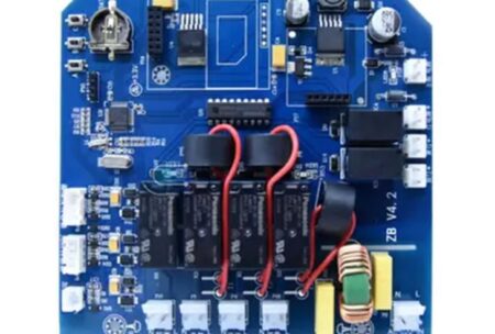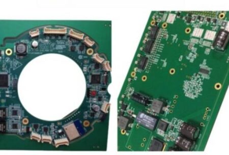

As electronic systems transmit more data through increasingly compact circuit boards, controlling crosstalk becomes an important challenge in high speed PCB manufacturing.
High-speed interfaces may route multiple signals through limited PCB space. When neighboring conductors interact electromagnetically, unwanted energy can couple from one signal path into another.
The result may include additional noise, degraded signal margins, or communication errors.
For OEM engineers developing networking equipment, computing hardware, and high-speed industrial electronics, crosstalk control requires coordinated decisions about routing, reference planes, layer assignment, and manufacturing tolerances.
What Causes Crosstalk on a High Speed PCB?
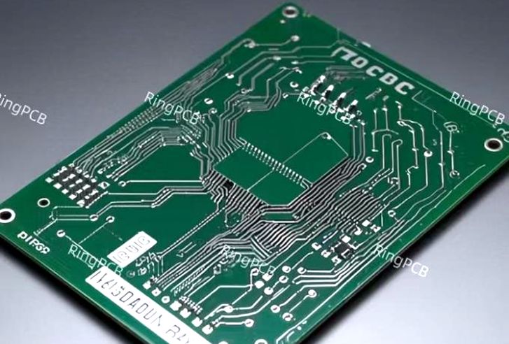
Crosstalk occurs when electromagnetic energy from one conductor couples into another conductor.
The source signal is commonly called the aggressor, while the affected signal is the victim.
Coupling can occur through electric fields and magnetic fields. Its severity depends on factors such as conductor spacing, parallel routing length, signal characteristics, and the surrounding PCB structure.
For example, two closely spaced traces routed in parallel over a long distance may couple more energy than traces that cross at a short distance.
However, spacing alone does not determine the outcome. Reference planes, dielectric properties, trace geometry, and signal transitions also influence coupling.
Consequently, crosstalk should be evaluated as part of the complete PCB interconnect design.
Separate Sensitive Signals From Aggressors
One practical way to manage crosstalk is to identify which signals are most sensitive to interference.
High-speed clock signals, fast digital interfaces, and low-level analog signals may require different routing considerations.
Where possible, engineers should avoid placing sensitive traces close to strong aggressors for long parallel distances.
Increasing separation can reduce coupling, but it may not be possible in densely routed designs.
In those cases, alternative routing layers, reference-plane arrangements, and more careful transition planning may provide additional control.
The appropriate approach depends on the signal requirements and available board area.
Rather than applying a universal spacing rule, engineering teams should define constraints based on the design’s electrical objectives.
Use Reference Planes to Support Signal Integrity
A continuous reference plane provides a return-current path for many high-speed signals and helps control electromagnetic behavior.
When a trace crosses a split or gap in its reference plane, the return current may need to take a less direct path.
This can increase loop area and contribute to unwanted electromagnetic coupling or other signal-integrity problems.
For multilayer boards, layer assignment should therefore consider both signal routing and reference-plane continuity.
A high-speed trace routed on one layer should have an appropriate reference structure for its intended impedance and signal characteristics.
When routing changes require layer transitions, engineers should evaluate the associated return-current path rather than checking only the signal trace itself.
Choose Layer Assignments Carefully
Multilayer PCB manufacturing provides additional routing layers, but more layers do not automatically guarantee better signal integrity.
The electrical benefit depends on how those layers are arranged and used.
For example, separating sensitive signal groups across suitable routing layers may reduce direct coupling.
However, adjacent signal layers without appropriate reference structures can still experience interlayer coupling.
The stackup should therefore be reviewed in terms of signal adjacency, reference planes, dielectric spacing, and the expected routing density.
For complex boards, these decisions should be evaluated before fabrication data is finalized.
A practical stackup balances signal-integrity requirements with manufacturing feasibility, mechanical constraints, and cost.
Understand Crosstalk Between PCB Layers
Crosstalk is not limited to neighboring traces on the same surface.
In multilayer boards, electric and magnetic fields can couple between conductors on different layers.
The degree of coupling depends on vertical spacing, routing overlap, reference-plane geometry, and other construction details.
This becomes particularly relevant when high-speed signals occupy closely spaced layers.
IPC technical literature has discussed interlayer crosstalk associated with PCB via structures and plane clearances, illustrating how manufacturing details and routing geometry can affect signal quality.
For demanding designs, engineers may need to evaluate layer-to-layer alignment and the geometry around plated through-holes.
Such considerations should be incorporated into the design and manufacturing review instead of being addressed only after signal-integrity problems appear.
Manage Via Transitions and Backdrilling Requirements
Vias introduce vertical interconnections between PCB layers.
Depending on the structure, an unused portion of a plated through-hole can behave as a stub and create an impedance discontinuity.
At sufficiently high frequencies, this may affect signal behavior.
Backdrilling can reduce certain via-stub effects, but it introduces additional manufacturing considerations.
The decision should depend on the signal’s operating range, the via structure, board thickness, and the required electrical performance.
OEMs should communicate any backdrilling or specialized via requirements clearly in the fabrication package.
The PCB manufacturer can then review the proposed structure, applicable tolerances, and inspection requirements before production.
Combine Simulation With Manufacturing Review
Simulation can help engineering teams identify potential crosstalk issues before committing to a final layout.
Depending on project complexity, analysis may include field-solver modelling, transmission-line simulation, or broader signal-integrity evaluation.
The results should be translated into practical design constraints, such as routing separation, stackup requirements, and acceptable impedance variation.
Manufacturing review is still necessary because the simulated structure must be physically achievable.
For example, a design that depends on extremely narrow spacing or tight registration tolerances should be reviewed against the manufacturer’s actual process capabilities.
Combining simulation and manufacturability assessment helps reduce the risk of designing an electrically desirable but difficult-to-produce board.
Define Validation Requirements Before Production
Crosstalk requirements should be connected to measurable electrical objectives.
Depending on the project, validation may include impedance measurements, time-domain reflectometry, or frequency-domain measurements of relevant interconnect structures.
The exact method depends on the design and the required acceptance criteria.
OEMs should specify which measurements are required, which structures will be tested, and what limits define acceptance.
Not every PCB order requires the same level of signal-integrity validation.
Clear requirements allow the manufacturer to determine the appropriate fabrication and verification scope before quoting.
High Speed PCB Manufacturing With Ring PCB
Founded in 2008, Ring PCB provides multilayer PCB manufacturing, PCB assembly, component sourcing, and full-turnkey PCBA services. Its published manufacturing capabilities include multilayer boards up to 62 layers, supporting projects that require complex routing structures.
For high-speed projects, customers can submit stackup details, Gerber files, controlled-impedance requirements, via specifications, and relevant manufacturing tolerances for review.
Ring PCB also supports rapid PCB prototyping in as little as 3 days for qualifying projects, subject to board complexity, material availability, and order requirements.

Effective crosstalk control depends on more than trace spacing. Routing topology, reference-plane continuity, layer assignment, via design, and manufacturing feasibility must work together.
By addressing these considerations before production, OEMs can make better-informed decisions when selecting a high speed PCB manufacturing partner.
To discuss your PCB requirements, contact rfq@ringpcb.com.
References
- IPC. Technical literature on signal integrity and interlayer crosstalk reduction.
- Ring PCB. About Ring PCB. https://www.ringpcb.com/about-us/