
Every NPI program has the same nightmare: the prototype measures clean, the design review is signed off, and the first volume lot comes back at 60% yield. The board did not change. The process window did.
That gap is getting more expensive to discover late. Boards engineered for 56–112 Gbps links already held about 41% of high-speed PCB revenue in 2025, and the 112 Gbps-plus segment is forecast to grow at roughly 18% CAGR. Those designs live inside insertion-loss budgets under 30 dB across a 30-inch trace, with via stubs specified below 5 mil and controlled impedance inside a few percent. Parameters that tight do not survive an unexamined handoff from a prototype line to a volume line.
Why Prototypes Pass and Volume Fails
Three mechanisms explain most of the gap.
Process windows differ by design. Prototype lines are built to reach limits; volume lines are built to repeat. A supplier may hold ±5% impedance in sample and ±10% in production, 0–8 mil backdrill stub in sample and 8–16 mil in series. Both numbers are honest. Only one of them ships.
Tolerance stacks compound. Registration, dielectric thickness, drill position and plating thickness each sit inside their own window. In series, drift between lots is normal and non-random, so margins that looked generous on ten panels can sit at the edge on a thousand.
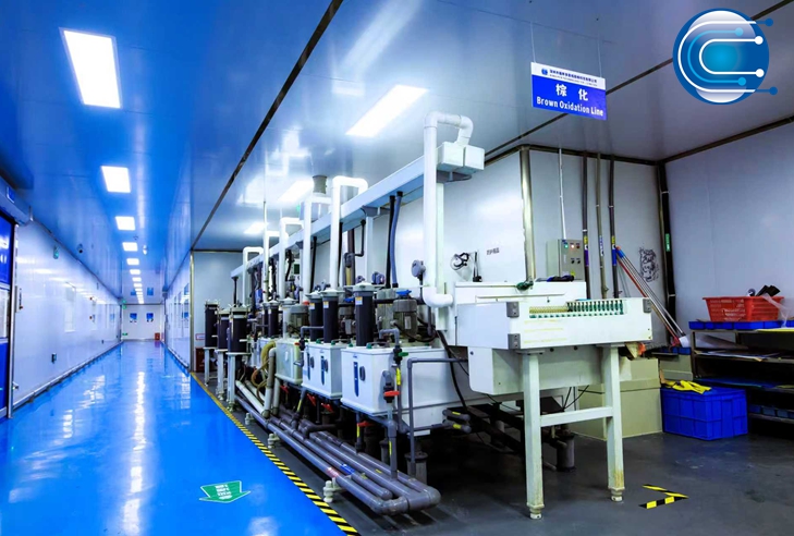
Learning does not transfer automatically. Prototype tooling, panelization, and operator attention are not the same assets as the volume line. If no one has reviewed the stack for the second environment, the second environment is unreviewed.
The Four Parameters That Decide the Transfer
1. Impedance. Confirm target value, tolerance and test coupon method at production, not only at sample. Ask how the fabricator compensates for dielectric thickness variation across the panel.
2. Via stub. A stub specification in mil is meaningless without a measurement method. Ask for the backdrill depth tolerance and how stub length is verified.
3. Microvia integrity. For HDI stacks, target pad capture, via taper and fill quality determine whether the board survives thermal cycling. Resin or copper paste fill with plating over fill (POFV) is the enabling step for via-in-pad, and it is a process discipline, not a purchase option.
4. Copper distribution. Heavy copper sections next to fine-line routing change etch behavior and plating uniformity. Mixed builds need explicit process notes, or the fine lines pay for the power section.
Have the DFM Conversation Before Gerber Release
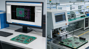
The most effective yield protection is a review that happens before fabrication, not after the first failed lot. What that review should surface: layers whose registration is marginal, drill schedules that exceed the production aspect ratio, impedance targets that depend on a single unavailable laminate, and finish choices incompatible with the assembly process downstream.
To be clear about scope: this is a manufacturability review of files already designed, not a design service. RingPCB works from your Gerber and BOM and reports what the process can and cannot hold.
How RingPCB Structures the Handoff
We keep the two capability columns explicit and quote both in the same document, so an NPI team can see exactly where a feature sits relative to the volume limit before tooling starts.
Sample line: 70 layers, 0.2–10 mm thickness, ±5% board thickness, 2.0/2.0 mil trace and space, 0.125 mm mechanical drills, 30:1 aspect ratio, laser vias 0.075–0.5 mm, ELIC HDI, 0–8 mil backdrill stub, ±5% impedance, 3 mil solder mask dam.
Volume line: 30 layers, 0.3–6.0 mm, ±10% thickness, 2.5/2.5 mil, 0.15 mm drills, 15:1 aspect ratio, laser vias 0.10–0.20 mm, 2+N+2 HDI, 8–16 mil stub, ±10% impedance, 4 mil solder mask dam.
Between those columns sits the entire NPI decision. A feature that lives only in the left column is a validation feature, and should be designed out or accepted as small-batch-only before the volume PO is raised.
Practical support around that structure: 72-hour rapid prototyping to shorten the loop, flexible small-batch runs to test the volume process without committing volume spend, mixed-material capability across FR-4, high-Tg and Rogers or Taconic RF laminates, and PCBA assembly with component sourcing so the assembly process is validated on the same panel that will ship.
The Realistic Goal
Aim for a transfer that fails loudly at prototype instead of quietly at volume. That means writing sample and volume capability into the purchase specification, requesting the manufacturability notes with the quotation, and running the first series lot small enough to learn from the result.
If your board is above 20 layers, uses microvias under 0.1 mm, needs a stub below 8 mil, or carries a loss budget under 30 dB, include those four numbers in your RFQ. We will answer them in two columns.
Send your Gerber files and BOM to rfq@ringpcb.com for a producibility review and quotation.
References:
- Mordor Intelligence, High-Speed PCB Market
- Emergen Research, AI Server HDI PCB Market
- SpecForge, PCB Demand 2026–2030