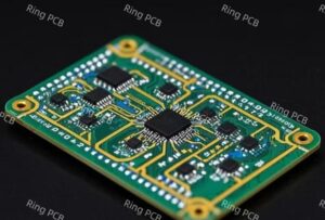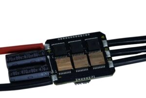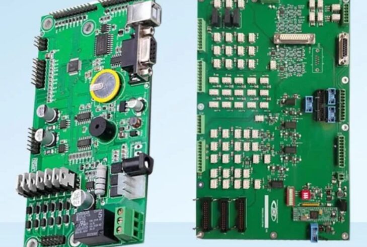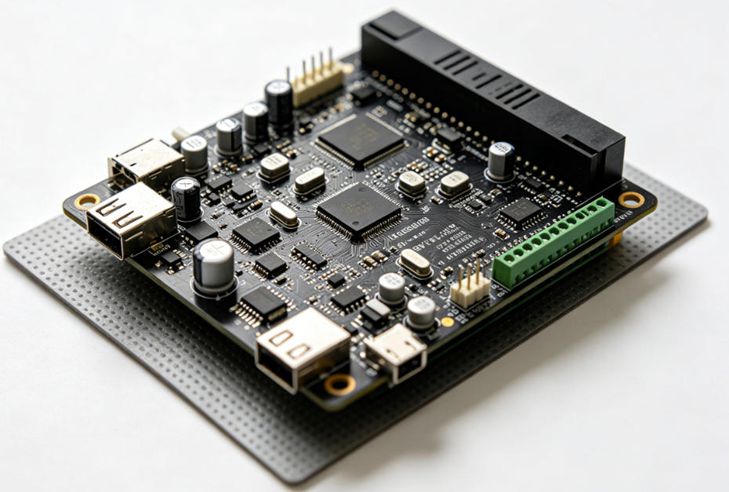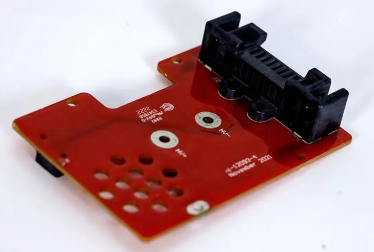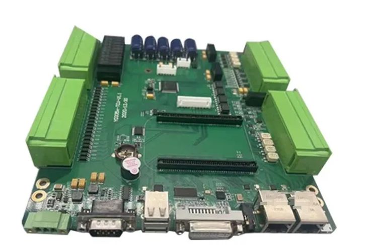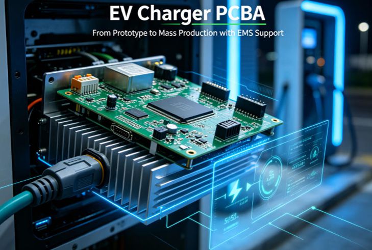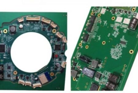
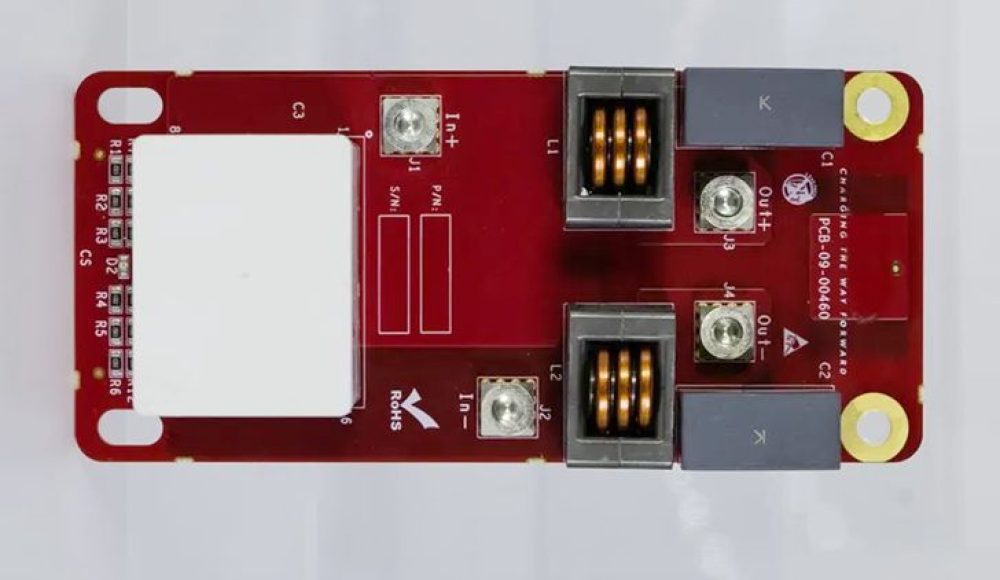
The rapid development of electric vehicles is increasing demand for reliable charging infrastructure. From residential AC wallboxes to commercial DC fast-charging stations, every charging system depends on electronic assemblies that control power conversion, monitor operating conditions, manage communication, and support electrical protection.
An EV charger PCBA is more than a collection of electronic components mounted on a circuit board. It must operate within a system exposed to high voltage, substantial current, switching noise, temperature variation, and, in many installations, outdoor environmental conditions. Consequently, PCB fabrication and assembly decisions can influence product safety, operating stability, and long-term service life.
For EV charger manufacturers and electronics procurement teams, choosing an appropriate PCBA manufacturing partner requires a clear understanding of the board’s electrical requirements and production risks. This article explains the major considerations when developing and manufacturing EV charger PCB assemblies.
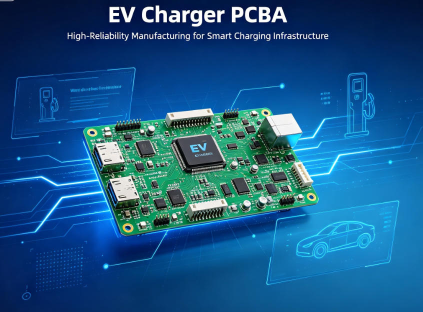
1. Understanding the Main Types of EV Charger PCBA
EV charging equipment contains several electronic subsystems. Their functions and manufacturing requirements can differ considerably.
AC EV Charger Control PCBA
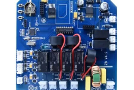
AC charging equipment commonly includes control and monitoring circuits, contactor drivers, current sensing, protection monitoring, and communication interfaces. These assemblies coordinate charging operations and communicate relevant status information to the vehicle or charging management system.
DC Fast Charger Power PCBA
DC fast chargers use power conversion modules to convert incoming electrical energy into controlled DC output. Their electronic assemblies may include power-factor-correction control, isolated DC/DC converter control, gate-driver circuits, current and voltage sensing, and thermal monitoring.
Communication and User Interface PCBA
Communication boards support functions such as charger networking, user authentication, display control, and communication with external systems. Depending on the product architecture, interfaces may include CAN, Ethernet, RS-485, wireless communication, or other protocols.
Auxiliary Power PCBA
Auxiliary power boards provide regulated supplies for control circuits, sensors, displays, communication modules, and other low-voltage subsystems.
Because these boards perform different functions, they should not automatically share identical PCB materials, assembly processes, or inspection requirements.
2. High-Voltage Isolation and PCB Layout Considerations
Electrical isolation is one of the most important design considerations in EV charger electronics.
High-voltage circuits and low-voltage control circuits may coexist within the same assembly. The PCB layout must therefore maintain appropriate separation between conductive regions according to the equipment’s operating conditions and applicable safety requirements.
Two important terms are:
- Clearance: The shortest distance through air between conductive parts.
- Creepage: The shortest distance along an insulating surface between conductive parts.
The required distances cannot be determined from nominal voltage alone. They may depend on working voltage, transient conditions, insulation category, pollution degree, material properties, altitude, and the applicable product standard.
During the manufacturing review, the supplier should understand the specified isolation boundaries and ensure that the fabrication data does not unintentionally compromise them. Slots, cutouts, connector positions, component footprints, and copper clearances may all affect the final construction.
However, the responsibility for the product’s electrical safety architecture and regulatory compliance remains with the equipment manufacturer and design authority. PCB fabrication and assembly should follow the approved design and documented requirements.
3. Managing High Current and Copper Requirements
EV charger power circuits may carry substantial current, especially within DC conversion and distribution sections. PCB copper thickness, trace width, plane geometry, connector selection, and current-path length all influence electrical and thermal performance.
Heavy copper PCB construction can provide additional copper cross-sectional area for high-current paths. Ring PCB’s published process capabilities list maximum inner and outer copper weights of 12 oz for mass production and 20 oz for samples. These are process capability limits, not a recommendation that every EV charger board should use the maximum copper weight.
The appropriate copper structure depends on current, allowable temperature rise, board thickness, trace geometry, cooling conditions, and manufacturing constraints.
In addition, high-current connections should be reviewed at component pads, terminals, plated through-holes, and connector interfaces. A wide copper trace alone does not guarantee a reliable current path if the connection points or solder joints become thermal bottlenecks.
4. Thermal Management for Continuous Charging Operation
Charging equipment may operate for extended periods, making thermal management a key reliability concern.
Heat can be generated by power semiconductors, rectifiers, inductors, transformers, current-sensing components, and high-current copper paths. If heat is not transferred efficiently, local hot spots may accelerate component aging or place excessive stress on solder joints and PCB materials.
Several design and manufacturing factors deserve attention:
Copper distribution: Appropriate copper planes and copper thickness can help spread heat, although the overall thermal path must also be considered.
Thermal vias: Arrays of plated vias may transfer heat between layers and toward a thermal plane or heat-spreading structure.
Component placement: High-power components should be positioned with the intended cooling method and mechanical structure in mind.
Solder joint quality: Large components and high-mass terminals may require careful control of solder paste, thermal profiles, and through-hole soldering conditions.
Mechanical interface: Heat sinks, mounting hardware, thermal pads, and enclosure contact surfaces should be considered as part of the complete assembly.
The final thermal performance must be validated at system level under the intended load and environmental conditions.
5. Component Selection and Mixed-Technology Assembly
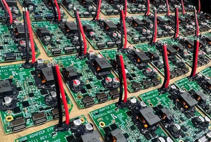
EV charger PCBAs often combine fine-pitch control components with large capacitors, inductors, connectors, relays, and power devices. This creates assembly challenges that differ from those of a board populated mainly with small surface-mount components.
SMT is suitable for many control ICs, resistors, capacitors, and other surface-mount devices. Through-hole assembly may be required for large connectors, terminals, transformers, and components that need additional mechanical support.
A mixed-technology board therefore requires coordinated SMT and through-hole processes.
Before production, the BOM should be reviewed for package compatibility, component availability, alternative part approvals, polarity, temperature ratings, and mechanical requirements. Large or heavy components should receive particular attention because their solder joints may experience mechanical and thermal stress during operation.
Where substitutions are necessary, the customer should approve the proposed alternatives before purchasing or assembly.
6. Environmental Protection and Long-Term Reliability
Many EV chargers are installed in parking areas, commercial sites, transport facilities, and other locations where equipment may encounter humidity, dust, temperature cycling, or corrosive contaminants.
The protection strategy may involve enclosure design, suitable surface finishes, conformal coating, sealing, and appropriate component selection.
For PCB assembly, coating or potting requirements should be clearly specified. The customer and manufacturer should agree on coating material, coverage areas, keep-out zones, masking requirements, and inspection criteria. Coating should not be assumed to compensate for inadequate PCB creepage or clearance design.
Similarly, solder joints and connectors should be evaluated according to the expected vibration, thermal cycling, and operating environment.
7. Inspection and Production Quality Requirements
A reliable EV charger PCBA program needs documented inspection and acceptance criteria.
Depending on the board design and customer requirements, the production plan may include solder paste inspection, automated optical inspection, X-ray inspection for selected hidden solder joints, visual inspection, and electrical or functional testing.
These methods serve different purposes. For example, visual inspection evaluates observable assembly workmanship, while X-ray may help assess certain hidden solder connections. Neither method alone establishes complete product safety or operating performance.
IPC J-STD-001 provides requirements for soldered electrical and electronic assemblies, while IPC-A-610 provides acceptance criteria for electronic assemblies. The applicable class, revision, and additional customer requirements should be agreed before production.
For EV charging equipment, the product manufacturer must also define the system-level safety, electrical, thermal, and regulatory validation plan.
8. Choosing an EV Charger PCBA Manufacturing Partner
Before placing an order, procurement teams should evaluate whether a supplier can support the board’s actual manufacturing requirements.
Useful questions include:
- Can the supplier manufacture the required PCB layer count and copper weight?
- Does it support both SMT and through-hole assembly?
- Can it review the BOM and discuss component availability?
- Are high-voltage isolation requirements clearly documented?
- Can inspection criteria be agreed before production?
- Are prototype and mass-production requirements evaluated separately?
- How are engineering changes and component substitutions communicated?
A supplier’s general assembly capacity is not enough. The production plan must be appropriate for the specific power, control, and communication boards involved.
EV Charger PCB and PCBA Manufacturing with Ring PCB
Ring PCB provides PCB fabrication, component sourcing, SMT assembly, through-hole assembly, and production quality inspection for electronics manufacturers. Its process capabilities include multilayer and heavy-copper PCB production, with published maximum copper weights of 12 oz for mass production and 20 oz for samples.
For EV charger projects, these capabilities may support the manufacturing requirements of power boards, control boards, and other electronic assemblies, subject to technical review. Ring PCB’s manufacturing team can review customer-provided Gerber files, BOM data, stackup details, and specific technical requirements before confirming project feasibility.
For a quotation or manufacturing discussion, contact rfq@ringpcb.com.
References and Further Reading
- IEC — IEC 61851 Series: Electric Vehicle Conductive Charging Systems.
- IEC — IEC 62196 Series: Plugs, Socket-Outlets, Vehicle Connectors and Vehicle Inlets.
- IEC — IEC 60664-1: Insulation Coordination for Equipment Within Low-Voltage Systems.
- IPC — IPC J-STD-001: Requirements for Soldered Electrical and Electronic Assemblies.
- IPC — IPC-A-610: Acceptability of Electronic Assemblies.
- U.S. Department of Energy — Alternative Fuels Data Center, Electric Vehicle Charging Infrastructure.