Introduction
The rapid expansion of 5G infrastructure, fiber-optic networks, data centers and high-speed communication systems is increasing the performance requirements of electronic hardware. Network switches, optical communication modules, base station equipment and industrial communication devices must process larger volumes of data while maintaining stable operation, low signal loss and consistent electrical performance.
For OEMs and electronics engineers, these requirements make Communication PCBA manufacturing more demanding than conventional electronic assembly. A reliable communication product depends not only on circuit board specifications but also on material selection, PCB fabrication quality, component sourcing, assembly precision and inspection throughout production.

As a result, choosing a manufacturing partner with both PCB fabrication and PCBA capabilities can help reduce coordination risks and improve production consistency.
1. Higher Data Rates Require More Careful PCB Material Selection
One of the most important considerations in communication electronics is signal transmission performance. As operating frequencies and data rates increase, signal attenuation, dielectric loss and impedance variation can become more significant.
Standard FR-4 materials remain suitable for many communication products. However, high-speed or high-frequency applications may require materials with more controlled dielectric properties and lower signal loss.
When evaluating PCB materials, engineers and procurement teams should consider:
- Dielectric constant (Dk): Affects signal propagation speed and impedance.
- Dissipation factor (Df): Influences dielectric loss, particularly at higher frequencies.
- Glass transition temperature (Tg): Relevant to thermal stability during fabrication and assembly.
- Thermal expansion: Affects dimensional stability and reliability under temperature changes.
- Material availability: Specialty laminates may have longer procurement lead times than standard FR-4.
The appropriate material depends on the product’s frequency range, stackup, operating environment and cost target. Selecting a premium laminate without considering actual electrical requirements can increase manufacturing costs without delivering meaningful benefits.
Therefore, material selection should be reviewed together with the PCB stackup, fabrication process and assembly requirements.
2. Multilayer PCB Fabrication and Impedance Consistency
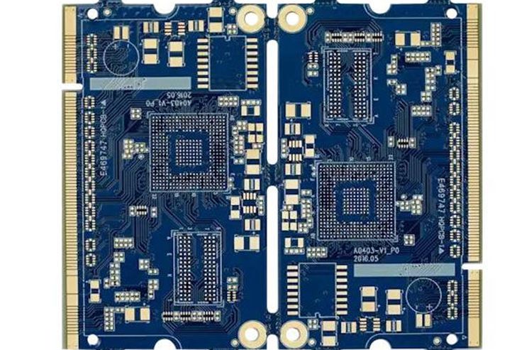
Communication equipment frequently uses multilayer PCBs to accommodate dense routing, power distribution, grounding and high-speed signal paths.
As layer count increases, manufacturing becomes more sensitive to layer registration, lamination parameters, drilling accuracy and copper plating consistency. Small variations can affect finished board dimensions, interlayer connections and electrical performance.
Controlled impedance is particularly important for high-speed communication interfaces. The target impedance must be supported by a suitable combination of trace geometry, copper thickness, dielectric thickness and material properties.
For OEM buyers, it is useful to confirm whether a PCB manufacturer can:
- Review stackup information and impedance requirements before production.
- Maintain consistent dielectric and copper thickness.
- Control layer-to-layer registration during lamination.
- Verify plated through-hole quality and interlayer connectivity.
- Provide inspection records and electrical test results where required.
These checks help identify manufacturing risks before boards enter assembly.
3. SMT Assembly for Dense Communication Electronics
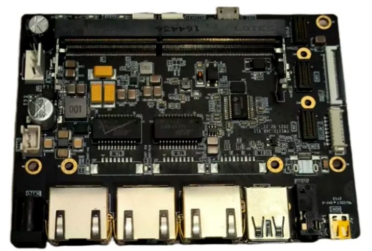
Communication products often contain fine-pitch ICs, processors, memory devices, RF components, connectors and power-management components. Their placement and soldering quality directly influence product performance.
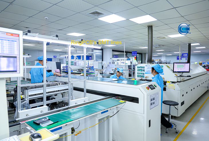
Surface Mount Technology (SMT) is widely used because it supports high component density and automated production. However, successful SMT assembly requires more than accurate component placement.
Key process controls include solder paste printing, stencil condition, component placement accuracy, reflow temperature profiling and solder joint inspection.
For example, fine-pitch components may be vulnerable to insufficient solder, bridging or inconsistent wetting. Large connectors and components with different thermal characteristics may require careful thermal profiling to achieve reliable solder joints.
A capable PCBA manufacturer should establish process parameters according to the actual PCB design, component package types and assembly requirements. First Article Inspection (FAI) can also help verify component placement, polarity, orientation and workmanship before volume production proceeds.
4. Component Sourcing and Supply Chain Coordination
Communication equipment may use specialized semiconductors, RF components, high-speed connectors and other parts with different availability and lifecycle characteristics.
A shortage or discontinuation of a critical component can delay an entire production schedule, even when PCB fabrication capacity is available.
Procurement teams should therefore evaluate component sourcing as part of the PCBA manufacturing process.
Important practices include:
- Confirming manufacturer part numbers and approved suppliers.
- Reviewing component lifecycle and obsolescence risks.
- Checking availability before committing to production dates.
- Maintaining traceability for purchased components.
- Reviewing proposed alternatives before making substitutions.
Unauthorized component substitutions should be avoided. Any alternative should be evaluated against the customer’s electrical, mechanical and regulatory requirements and approved through the agreed change-control process.
5. Inspection and Testing for Consistent Production Quality
Communication PCBA quality cannot be assessed through visual appearance alone. Different inspection methods identify different types of manufacturing defects.
Automated Optical Inspection (AOI) checks visible assembly features, including component presence, polarity, alignment and certain soldering defects.
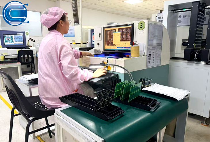
X-Ray inspection is useful for examining hidden solder joints, such as those beneath Ball Grid Array (BGA) packages.
Electrical testing can help identify open circuits, short circuits and connectivity issues. Additional functional testing may be required depending on the product and customer test specifications.
Inspection plans should be determined by product complexity, component packages, quality risks and customer requirements. No single inspection method can identify every possible defect.
6. Planning for Scalable Communication PCBA Production
A communication product that performs well during prototype testing may still encounter manufacturing challenges when production volume increases.
Before mass production, OEMs should review material availability, assembly yield, test coverage, production capacity and change-control procedures. Pilot runs and first-article verification can help expose process issues before larger orders are released.
Early communication between the OEM and manufacturer is particularly important when a project includes complex multilayer boards, fine-pitch components or specialized materials.
How Ring PCB Supports Communication Electronics Manufacturing
Ring PCB provides integrated PCB fabrication and PCBA manufacturing services for customers developing communication and other electronic products.
Founded in 2008, Ring PCB operates a 10,000+ sqm self-owned manufacturing facility with approximately 500 employees. Its capabilities include PCB fabrication of up to 62 layers, five automated SMT production lines, component sourcing, through-hole assembly, inspection and testing.
With monthly bare PCB production capacity of approximately 50,000 sqm and the ability to handle around 500 PCBA projects per month, Ring PCB supports different project scales and manufacturing requirements. Rapid PCB prototypes can be available in as little as three days, subject to project specifications and material availability.
Customers can submit Gerber files, BOM data and detailed technical requirements for manufacturing review. The Ring PCB team can then communicate with customers to assess production requirements and feasibility before order confirmation.
Conclusion
Reliable communication PCBA manufacturing requires coordination across material selection, multilayer PCB fabrication, SMT assembly, component sourcing and inspection. As communication systems demand higher data rates and more compact hardware, manufacturing consistency becomes increasingly important.
By evaluating these factors early and working with a capable manufacturing partner, OEMs can reduce production risks and build a more stable path from prototype to volume manufacturing.
For communication PCB and PCBA manufacturing inquiries, contact Ring PCB:
Email: rfq@ringpcb.com
References and Further Reading
- Grand View Research – Printed Circuit Board Market
- KBV Research – High-Speed PCB Market
- Global Electronics Association – Supply Chain Availability, August 2026: