1. Why Industrial Control Equipment Needs Heavy Copper PCBs
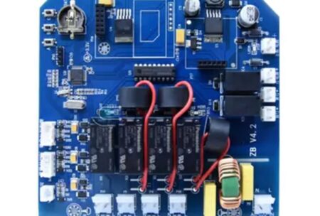
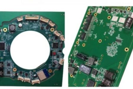
Industrial control equipment often combines low-power control circuits with high-current power stages. Motor drives, servo controllers, industrial inverters and power distribution systems must manage electrical loads while maintaining stable operation over extended production cycles.
As industrial automation becomes more sophisticated, electronic control systems are also expected to deliver greater functionality and power performance within practical equipment dimensions.
Cisco’s 2026 industrial research shows that AI adoption is moving into live industrial operations, increasing requirements for connected machines, reliable infrastructure and real-time processing. Although this trend is not limited to power electronics, it reflects the broader shift toward more capable industrial equipment and increasingly demanding electronic systems. [Source: Cisco, 2026 State of Industrial AI Report.]
In power-related industrial applications, PCB construction is particularly important. Standard copper thickness may not always provide the conductor cross-section required by a high-current circuit.
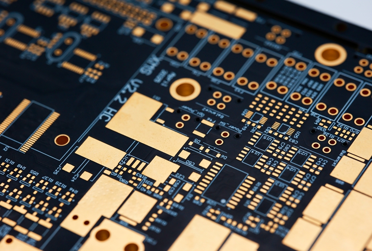
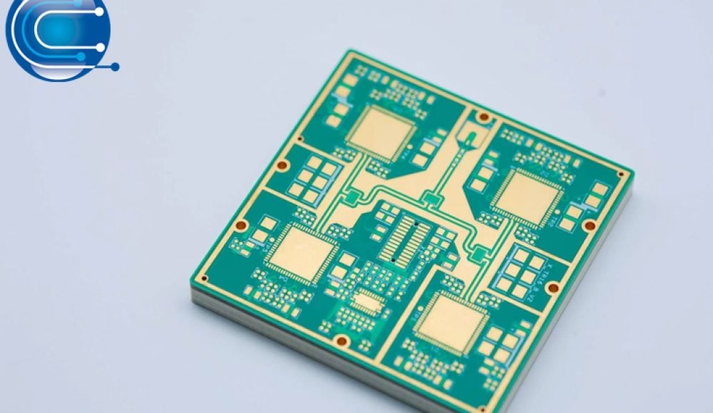
A Heavy Copper PCB uses thicker copper layers to support demanding current paths and improve heat spreading in suitable applications. When combined with appropriate component selection and assembly processes, it can serve as a practical platform for industrial power control electronics.
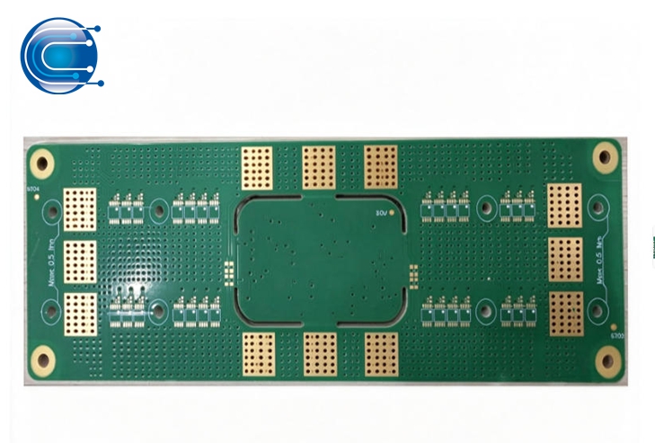
However, a heavy copper board is not simply a standard PCB with thicker copper. Its construction affects fabrication, component soldering, inspection and the overall PCBA manufacturing process.
2. Industrial Control Applications That Benefit from Heavy Copper PCB Assembly
Heavy copper PCB technology is most relevant to industrial control products where the board carries substantial current or connects power components.
Industrial Motor Drives
Motor drives regulate the speed and torque of industrial motors used in conveyors, pumps, compressors and production machinery.
Their electronic assemblies may include power semiconductors, gate drivers, current-sensing circuits and control processors.
Heavy copper layers can provide more substantial conductor paths for power circuits. They may also help distribute heat across selected copper areas, depending on the board construction and thermal design.
Servo Drives and Motion Control Equipment
Servo systems require precise motor control and power conversion. Their PCBA may combine low-level feedback signals with high-current switching circuits.
The PCB must accommodate both sensitive control electronics and power-related components. Copper distribution, component placement and electrical separation are important considerations when selecting the board structure.
Industrial Inverters and Power Conversion Systems
Industrial inverters convert electrical power for motor control and other equipment applications. Their PCB assemblies may contain switching devices, capacitors, power connectors and control circuits.
Heavy copper can be used in selected power layers to support current-carrying requirements. The actual copper thickness should be determined by current, trace geometry, allowable temperature rise and manufacturing feasibility.
Industrial Power Distribution and Energy Equipment
Power distribution modules and industrial energy systems may require robust PCB conductor paths for current transfer between components and terminals.
Depending on the electrical and mechanical requirements, heavy copper constructions can provide an alternative to conventional copper structures or selected busbar arrangements.
3. What Heavy Copper Changes in Industrial PCBA Manufacturing
The benefits of heavy copper are closely connected to its manufacturing requirements. For PCBA buyers, understanding these differences is important when evaluating an assembly supplier.
Copper Thickness and PCB Fabrication
Thicker copper changes the etching process and the geometry of finished conductors.
As copper thickness increases, achieving fine trace widths and narrow spacing becomes more challenging. The manufacturer must consider etching compensation, conductor dimensions and the required insulation distances.
For industrial control PCBA, the fabrication data should clearly identify the copper weight for each relevant layer. Inner and outer layers may have different copper requirements.
Solder Pad and Component Footprint Compatibility
Heavy copper boards are often used with power components such as MOSFETs, IGBTs, power diodes, terminals and large capacitors.
Their pad dimensions and thermal characteristics may differ significantly from those of small signal components.
The assembly process must account for the component footprint, solder paste volume, stencil design and thermal behavior during reflow or other soldering processes.
Thermal Behavior During Soldering
Thick copper has a greater capacity to absorb and distribute heat than thinner copper structures. During soldering, this can influence how quickly different areas of the PCB reach the required temperature.
Large copper areas connected to component pads may draw heat away from solder joints. If the reflow profile is not suitable, this can contribute to inconsistent wetting or incomplete soldering.
Therefore, the assembly team should evaluate the board construction and component distribution when establishing the soldering process.
Mechanical and Connection Requirements
Industrial power assemblies may use large connectors, screw terminals and heavy components. Their mechanical loads can affect solder joints and PCB mounting areas.
The board should be reviewed for connector support, mounting positions, copper balance and mechanical stress.
For products exposed to vibration, the customer and manufacturer should also agree on any additional mechanical or assembly requirements.
4. Key Quality Control Points for Heavy Copper PCBA
Heavy copper PCB assembly requires inspection beyond simply confirming that components are correctly placed.
Several process stages deserve particular attention.
Incoming PCB Inspection
The incoming board should be checked against the approved fabrication requirements. Relevant items include board thickness, copper specifications, surface finish, conductor condition, hole quality and dimensional requirements.
Solder Paste Printing and SPI
Power components may have large pads or thermal pads that require carefully controlled solder paste deposition.
Solder Paste Inspection (SPI) helps verify paste volume, position and printing consistency before components are placed.
Component Placement and Reflow
Large power components and small control components can behave differently during assembly. Placement accuracy and a suitable thermal profile are important for achieving consistent solder joints.
The reflow process should be validated against the actual board construction and component requirements rather than relying on a generic temperature profile.
AOI and X-Ray Inspection
AOI can identify visible assembly defects, including component misalignment, polarity issues and soldering abnormalities.
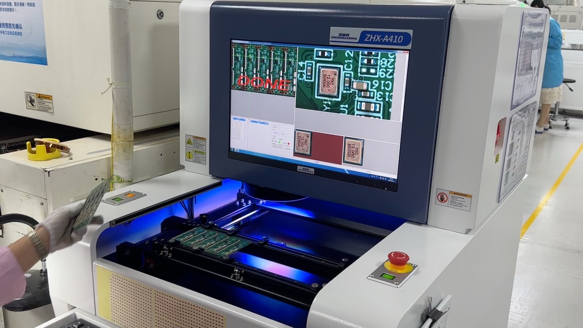
For packages with hidden solder connections, X-ray inspection can provide additional visibility into solder joint conditions.
The inspection scope should be selected according to the component types and the customer’s quality requirements.
Electrical and Functional Verification
Where specified in the project scope, electrical testing and functional verification can help confirm that the assembled board meets the agreed requirements.
For industrial power control boards, test plans may cover power input, output behavior, control signals and other application-specific functions. These tests should be defined with the customer and should not be assumed to be identical for every PCBA project.
5. How to Select the Right Heavy Copper Construction
More copper does not necessarily mean a better PCB. The appropriate construction depends on the electrical load, physical dimensions, thermal conditions and production cost.
Before choosing a heavy copper PCB, OEM engineering teams should review the following factors.
- Operating current: Determine the continuous and peak current requirements for each power path.
- Copper weight: Select copper thickness according to conductor dimensions, electrical requirements and acceptable temperature rise.
- Trace width and spacing: Confirm that the required geometry can be manufactured consistently with the selected copper thickness.
- Layer distribution: Evaluate whether power and control circuits should use separate layers or dedicated routing areas.
- Thermal conditions: Consider component heat generation, board temperature, airflow and available heat dissipation paths.
- Assembly requirements: Review component footprints, soldering conditions, connectors and mechanical support.
In some industrial control applications, a combination of standard-copper signal layers and heavier-copper power layers may be more practical than using heavy copper throughout the entire board.
This approach can help balance power handling, routing flexibility, assembly requirements and manufacturing cost.
6. What Industrial OEMs Should Provide for a Heavy Copper PCBA Quote
A reliable quotation depends on more than board dimensions and order quantity.
To support an accurate manufacturing review, customers should prepare:
- Gerber files and PCB fabrication specifications
- Copper weight requirements for individual layers
- Stackup and finished board thickness
- Current and voltage requirements for relevant circuits
- BOM and component specifications
- Pick-and-place files and assembly drawings
- Required inspection and testing standards
- Prototype and production quantities
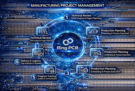
Providing these details early allows the manufacturer to review fabrication feasibility and identify potential assembly issues before production.
7. Heavy Copper PCB Manufacturing and Assembly at Ring PCB
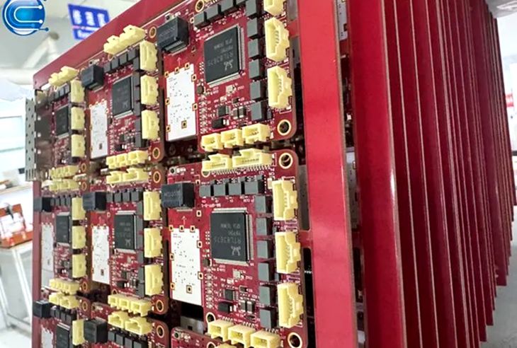
Ring PCB provides PCB fabrication, component sourcing, SMT assembly and through-hole assembly for industrial electronics and power-related applications.
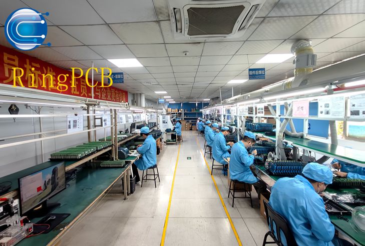
Established in 2008, Ring PCB operates a self-owned manufacturing facility covering more than 10,000 square meters. Its production capabilities include multilayer PCB manufacturing, heavy copper PCB fabrication and integrated PCBA services.
According to its published process capability information, Ring PCB supports:
- Inner and outer copper up to 12 oz for mass production
- Copper up to 20 oz for sample projects
- Up to 30 layers for mass production and up to 70 layers for samples
- Specialized PCB constructions for demanding electrical and manufacturing requirements
Actual feasibility depends on board dimensions, copper distribution, trace geometry, layer structure, materials and order conditions.
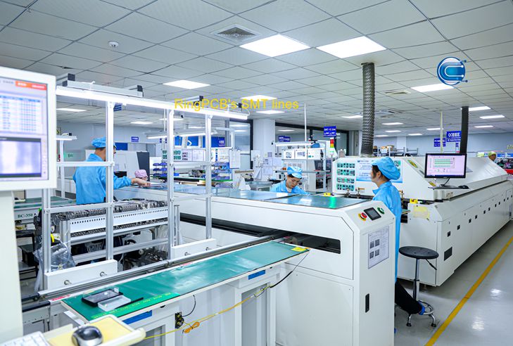
For PCBA projects, Ring PCB provides component sourcing, SMT and through-hole assembly, together with production inspection using SPI, AOI and X-ray equipment. These processes support manufacturing control for industrial control boards with different component and assembly requirements.
Customers can submit Gerber files, BOM information, copper specifications and assembly requirements for technical communication and manufacturing feasibility review.
If you are looking for a heavy copper PCB manufacturer or an industrial control PCBA partner, contact Ring PCB at rfq@ringpcb.com to discuss your project requirements.
References
- Cisco. (2026). 2026 State of Industrial AI Report.
- IPC. IPC-2221: Generic Standard on Printed Board Design.
- IPC. IPC-6012: Qualification and Performance Specification for Rigid Printed Boards.
- Ring PCB. Heavy Copper PCB: How to Improve Current Capacity and Thermal Performance. https://www.ringpcb.com/heavy-copper-pcb-current-capacity-and-thermal-design-2/
- Ring PCB. Ring PCB Process Capabilities: From Prototyping to Mass Production. https://www.ringpcb.com/ringpcb-process-capabilities-from-prototyping-to-mass-production/