1. Why Industrial Control Systems Need Higher-Density PCBs
Industrial automation is evolving beyond conventional programmable logic controllers and standalone machine controls. Modern equipment increasingly integrates real-time monitoring, machine vision, industrial networking, edge computing and intelligent motion control. As a result, control electronics must accommodate more processing functions and communication interfaces within increasingly compact enclosures.
Cisco’s 2026 State of Industrial AI research highlights this shift. Its survey found that 61% of industrial organizations were already using AI in live industrial operations, while 97% expected AI workloads to affect their industrial network requirements. These developments place greater demands on the electronic systems supporting connected machines and intelligent factory operations. [Source: Cisco, 2026 State of Industrial AI Report.]
For PCB and PCBA manufacturers, one practical consequence is the growing need to accommodate more components, signal connections and functional modules within limited board space.
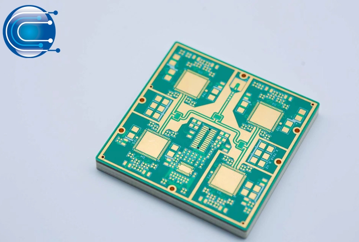
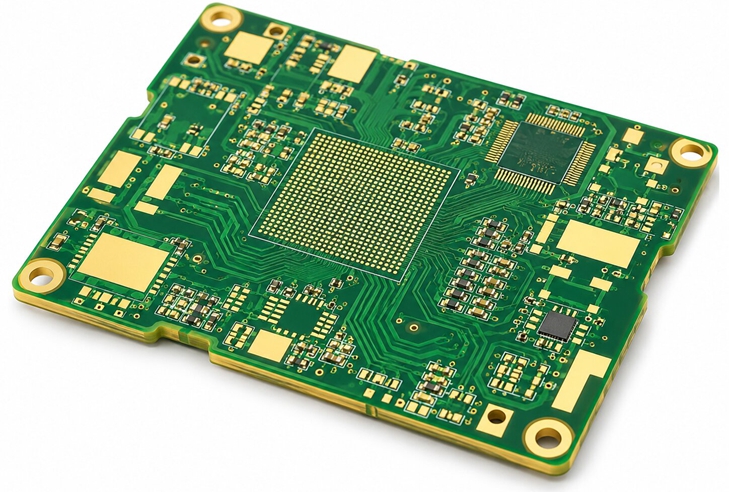
This is where High-Density Interconnect (HDI) PCB technology becomes relevant to industrial control PCBA manufacturing. By using finer conductor patterns, laser-drilled microvias and advanced interconnection structures, HDI PCBs can provide greater routing density than conventional multilayer boards.
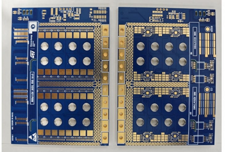
However, HDI is not automatically the best solution for every industrial controller. Its value depends on the component layout, routing complexity, product dimensions and manufacturing requirements.
2. Where HDI PCB Technology Fits in Industrial Control Equipment
HDI technology is particularly relevant when industrial control products combine compact dimensions with complex electronic functions.
PLCs and Compact Industrial Controllers
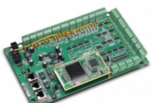
Modern PLCs and compact controllers may integrate processors, memory, communication interfaces, input/output circuits and signal-conditioning components on relatively small circuit boards.
When conventional through-hole routing becomes difficult to accommodate, HDI structures can provide additional routing channels. Blind vias and microvias allow selected layers to be interconnected without requiring every connection to pass through the entire board.
This can help engineers accommodate fine-pitch components and increase routing flexibility within a limited PCB footprint.
Industrial Robots and Motion Control Systems
Robotic controllers and motion-control electronics may require multiple processing, feedback and communication functions. Their circuit boards can contain high-pin-count components, sensors interfaces and control signal circuits.
HDI technology can support dense component arrangements and complex interconnections. This is particularly useful when the control unit must fit into a compact enclosure or integrate several electronic functions.
Nevertheless, the PCB structure must still be evaluated for electrical noise, thermal conditions and mechanical requirements associated with the equipment.
Industrial IoT and Edge Controllers
Industrial gateways and edge controllers connect sensors, machines and factory networks. Their PCBs may combine processors, memory, wired communication interfaces and wireless modules.
HDI can help accommodate these components without continuously increasing board dimensions. It may also provide more routing flexibility for products requiring multiple high-density component packages.
3. How HDI Structures Improve Industrial Control PCBA Integration
The primary advantage of HDI is not simply reducing board size. It is providing additional interconnection options for complex electronic assemblies.
Several manufacturing structures are especially relevant.
Laser-Drilled Microvias
Microvias provide short interconnections between selected PCB layers. Their smaller diameters can help release routing space around fine-pitch components and high-density component packages.
For industrial controllers using compact BGA packages, microvias can support more efficient fan-out routing when conventional via structures are insufficient.
Blind and Buried Vias
Blind vias connect an outer layer to selected inner layers, while buried vias connect internal layers without extending to the outer surfaces.
These structures can reduce the routing space consumed by conventional through-hole vias. They are useful when multiple signal layers must be interconnected within a limited board area.
Sequential Lamination and Build-Up Structures
HDI boards may use sequential lamination to create additional build-up layers. This allows manufacturers to combine conventional multilayer core structures with high-density interconnection layers.
The selected stackup must be evaluated according to layer count, dielectric thickness, via structure, material compatibility and manufacturing yield.
For industrial control PCBA, the objective is to obtain a manufacturable board construction that supports the required component layout and electrical performance.
4. Manufacturing Challenges When Assembling HDI Industrial Control PCBAs
Although HDI technology provides greater routing density, it also introduces additional manufacturing considerations.
Fine-Pitch Component Placement
HDI boards often accommodate fine-pitch BGAs, QFNs and other compact packages. These components require accurate solder paste printing, component placement and reflow control.
Solder paste volume must be appropriate for the pad dimensions. Excessive or insufficient paste can contribute to bridging, open joints or inconsistent solder connections.
SPI inspection can help verify solder paste printing before component placement, while AOI can identify visible assembly defects after soldering.
Microvia and Via-in-Pad Considerations
Via-in-pad structures can help increase routing density, but the via construction and surface condition must be suitable for component soldering.
Plated over filled vias (POFV) can provide a flatter surface for solder pad applications. The filling quality, plating integrity and surface flatness should be confirmed according to the agreed manufacturing requirements.
Inspection of Hidden Solder Joints
Fine-pitch BGA components contain solder joints that cannot be fully inspected through conventional visual methods.
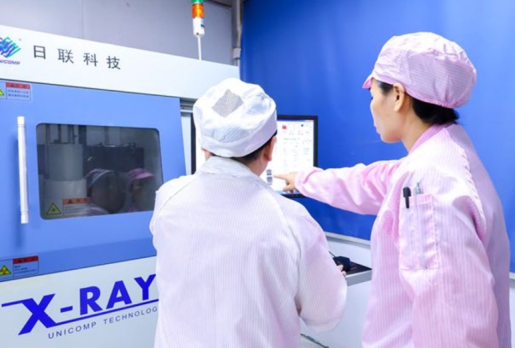 can help evaluate hidden solder connections, including potential voiding, bridging and other assembly concerns.
The inspection method and acceptance criteria should be determined according to the component package, product risk and customer quality requirements.
Thermal and Electrical Considerations
Industrial control boards may operate continuously and experience changing temperatures and electrical loads.
Although HDI improves routing density, a smaller PCB does not automatically provide better thermal performance. Component placement, copper distribution, power routing and heat dissipation paths must still be considered.
Manufacturers should review the complete PCB construction and assembly requirements rather than evaluating microvia dimensions alone.
5. When Should Industrial OEMs Consider HDI PCB Assembly?
HDI PCB assembly may be worth evaluating when a project has one or more of the following characteristics:
- High-pin-count BGA or fine-pitch components require additional fan-out routing.
- The control board must fit into a compact mechanical enclosure.
- Multiple processing and communication functions need to be integrated.
- Conventional multilayer routing cannot accommodate the required connections efficiently.
- Product miniaturization is a priority, but the required functionality must be maintained.
On the other hand, if a conventional multilayer PCB can meet the routing, electrical, mechanical and cost requirements, HDI may introduce unnecessary manufacturing complexity.
OEMs should therefore compare different PCB constructions based on the actual application instead of selecting HDI simply because it is a more advanced technology.
6. What Buyers Should Review Before Ordering HDI Industrial Control PCBA
Before selecting an HDI PCB assembly manufacturer, engineering and procurement teams should prepare the manufacturing information needed for a meaningful feasibility review.
Important items include:
- PCB fabrication data: Gerber files, stackup information, board dimensions and copper specifications.
- HDI construction: Build-up structure, microvia dimensions, blind and buried via requirements, and via filling specifications.
- Assembly documentation: BOM, component placement files and assembly drawings.
- Component requirements: Package types, fine-pitch components, BGA specifications and sourcing requirements.
- Quality requirements: Inspection methods, acceptance criteria and any customer-specific testing requirements.
Early communication between PCB fabrication and PCBA teams helps identify potential manufacturing issues before production begins.
7. HDI PCB Manufacturing and Industrial Control PCBA at Ring PCB
Ring PCB provides PCB fabrication, component sourcing and PCB assembly services for industrial electronics projects. Established in 2008, the company operates a self-owned manufacturing facility of more than 10,000 square meters and supports a range of multilayer and advanced PCB manufacturing requirements.
For HDI PCB production, Ring PCB’s published process capabilities include:
- 2+N+2 HDI structures for mass production
- ELIC capability for sample projects
- Laser microvia diameters of 0.10–0.20 mm for mass production
- Blind and buried via manufacturing
- POFV and other specialized interconnection processes
Actual feasibility depends on the complete board construction, material selection, dimensions and project requirements.
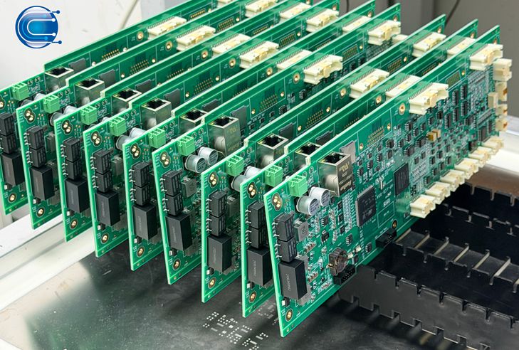
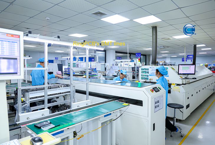
Ring PCB also provides SMT and through-hole assembly, component sourcing, and production inspection. Its five automated SMT lines support different PCBA production requirements, while SPI, AOI and X-ray inspection equipment support assembly quality control.
Customers can submit Gerber files, BOM information and specific technical requirements for manufacturing communication and feasibility review.
If you are sourcing an HDI PCB manufacturer for industrial controllers, automation equipment or compact electronic systems, contact Ring PCB at rfq@ringpcb.com to discuss your project.
References
- Cisco. (2026). 2026 State of Industrial AI Report. https://newsroom.cisco.com/c/r/newsroom/en/us/a/y2026/m03/state-of-industrial-ai-report-2026.html
- HKEX News. (2026). Industry Overview: Global High-Build-Up HDI PCB Market.
- IPC. IPC-2226: Sectional Design Standard for High Density Interconnect (HDI) Printed Boards.
- IPC. IPC-6016: Qualification and Performance Specification for High Density Interconnect (HDI) Structures.
- Ring PCB. HDI PCB Manufacturing: Microvias, Stackup and Reliability. https://www.ringpcb.com/hdi-pcb-manufacturing-microvias-stackup-and-reliability/