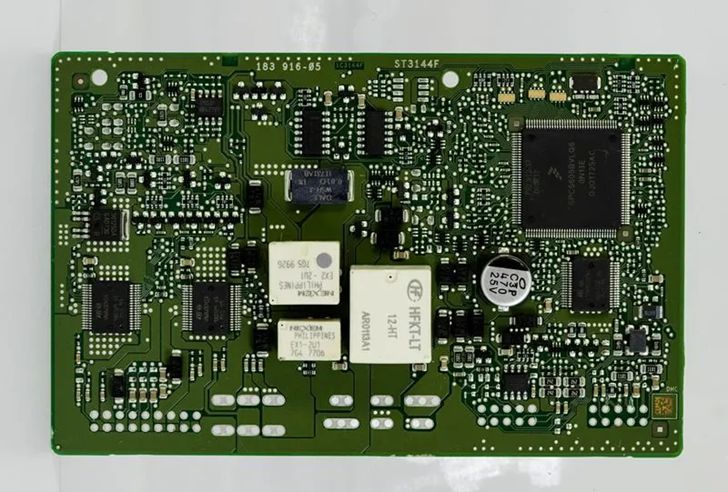
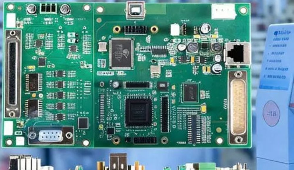
FR-4 is widely used in industrial control PCB manufacturing because it offers a practical balance of electrical insulation, mechanical strength, thermal properties and manufacturing cost. However, selecting the right material is only one part of preparing a PCB for production.
Even when a circuit board meets its electrical requirements, incomplete manufacturing files, unsuitable copper clearances, unclear drilling specifications or inconsistent layer information can create problems during fabrication. These issues may lead to additional technical clarification, production revisions, material waste and delivery delays.
For industrial OEMs, preparing a complete manufacturing data package before placing an order is an effective way to reduce these risks. This article outlines eight important checks for FR-4 industrial control PCB projects, from file preparation to production readiness.
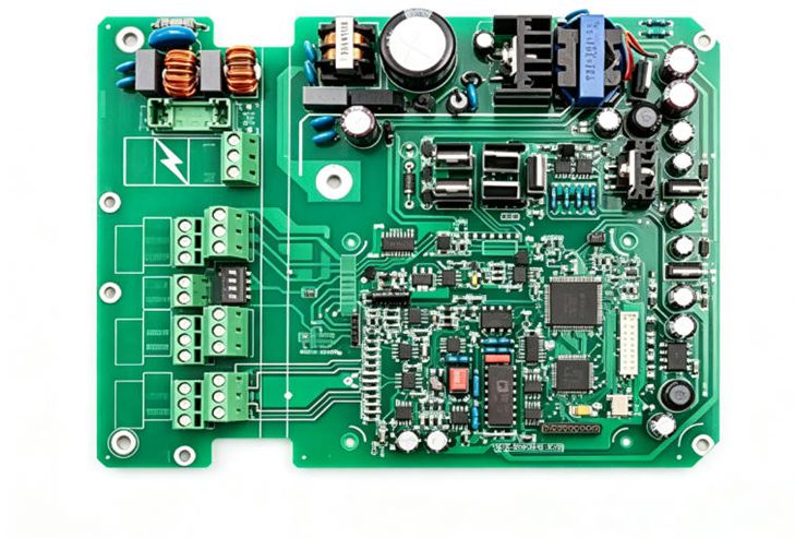
1. Confirm That the Gerber Files Are Complete
Gerber files provide the manufacturing information needed to reproduce the PCB’s copper patterns, solder mask, silkscreen and other board features.
Before submitting a project, check that the manufacturing package contains all required layers. Depending on the PCB construction, this generally includes:
- Copper layer data for each PCB layer
- Top and bottom solder mask files
- Silkscreen or legend files
- Board outline and routing information
- NC drill files
- Relevant fabrication notes and mechanical drawings
File naming is equally important. Each file should clearly identify its function, board part number and revision. For example, a file package containing multiple versions of the same board should make the approved production revision easy to identify.
Missing layers, unclear board outlines or mismatched drill information can delay the manufacturing review. Therefore, it is good practice to check the complete file package before requesting a quotation.
2. Specify the FR-4 Material and PCB Stackup
The term FR-4 does not describe one identical material specification. Different laminate grades may have different Tg, CTE, dielectric properties and thermal characteristics.
For industrial control applications, the selected material should match the product’s operating environment and manufacturing requirements.
The PCB documentation should identify relevant details such as:
- FR-4 material grade or required material properties
- Total board thickness
- Number of copper layers
- Copper weight for each layer, where specified
- Dielectric thickness and stackup requirements
- Controlled impedance requirements, if applicable
For multilayer boards, a clearly defined stackup is particularly important. The manufacturer needs to understand the intended layer arrangement and material construction before fabrication.
If the stackup is not fully specified, the customer and manufacturer should clarify the construction assumptions before production. This helps avoid differences between the intended electrical structure and the actual manufactured board.
3. Review Trace Width, Spacing and Copper Clearance
Copper geometry directly affects electrical connectivity and manufacturability.
Industrial control boards may contain low-level signal circuits alongside power and switching sections. Their copper requirements can vary significantly across the same board.
Important parameters include:
Minimum trace width: Traces must be wide enough for the required manufacturing process and electrical current. Power paths may require wider copper than signal traces.
Minimum spacing: Adequate clearance between copper features helps prevent unintended electrical shorts.
Copper-to-edge clearance: Copper positioned too close to the board edge may become exposed during routing or create edge-related manufacturing concerns.
Drill-to-copper clearance: Sufficient distance between drilled holes and nearby copper features helps prevent unwanted connections after plating.
Annular ring: Adequate copper around drilled holes is important for reliable plated through-hole connections.
These values should not be copied from a generic online checklist without checking the selected manufacturer’s actual process capabilities. Minimum feature sizes depend on board construction, material, copper thickness and production tolerances.
A manufacturing capability review helps determine whether the specified geometry can be produced reliably.
4. Check Hole Sizes, Via Structures and Aspect Ratio
Drilling and plating are important steps in multilayer PCB fabrication. Holes may be used for component mounting, mechanical fixing or electrical connections between copper layers.
For FR-4 industrial control boards, the manufacturing information should distinguish between:
- Plated through-holes
- Non-plated holes
- Via holes
- Mechanical mounting holes
- Special hole or slot requirements
Finished hole size and drill size are not necessarily the same because copper plating changes the final opening. The manufacturing drawing should make the required dimensions clear.
For multilayer boards, the relationship between board thickness and hole diameter also matters. A high hole aspect ratio can increase drilling and plating challenges.
When a board contains dense routing, small vias or complex interconnections, these details should be reviewed before production. Clear drilling data helps reduce the risk of incorrect hole sizes, insufficient clearances or plating-related problems.
5. Verify Solder Mask and Surface Finish Requirements
Solder mask protects exposed copper areas and helps define the solderable pads used during assembly. Incorrect solder mask openings can affect soldering quality, particularly around fine-pitch components and closely spaced pads.
Before production, confirm:
- Top and bottom solder mask coverage
- Solder mask openings around component pads
- Required mask color, if specified
- Solder mask clearance and dam requirements
- Any exposed copper areas or special mask instructions
Surface finish should also be selected according to component requirements, storage considerations and assembly processes.
Common PCB surface finishes include HASL, lead-free HASL, ENIG and OSP. Each has different characteristics and cost implications. The appropriate choice depends on the board’s application, component pitch, solderability requirements and production expectations.
For industrial control PCBs, it is important to specify the required finish clearly rather than leaving the choice open to assumptions.
6. Review Board Outline, Panelization and Mechanical Details
Mechanical information is sometimes overlooked when preparing PCB manufacturing files. However, board dimensions, cutouts, slots and edge requirements can influence fabrication, assembly and final product integration.
Check that the manufacturing package clearly identifies:
- Finished board dimensions and tolerances
- Board outline and routing paths
- Internal cutouts and slots
- Mounting holes and their positions
- Edge clearance requirements
- Any beveling or special mechanical processing
Panelization should also be considered when the production process requires multiple boards to be manufactured or assembled together.
For PCBA orders, panel design may influence handling, component placement near board edges, depanelization and assembly efficiency. The panelization method should be compatible with the manufacturer’s production equipment and the board’s mechanical characteristics.
Clear mechanical drawings help reduce the possibility of dimensional misunderstandings between the OEM and manufacturer.
7. Check BOM and Assembly Documentation Before PCBA Production
For projects that include PCBA manufacturing, PCB fabrication files are only part of the required information. The component and assembly documentation must also be consistent.

A complete assembly package may include:
- BOM with manufacturer part numbers
- Component reference designators
- Pick-and-place or centroid data
- Assembly drawings
- Component polarity and orientation information
- Special assembly instructions
- Inspection and testing requirements, where applicable
The BOM should be checked for missing part numbers, incorrect package descriptions and unclear component specifications.
For industrial electronics, component availability is another important consideration. Long-lead-time or end-of-life components can affect production schedules. Where alternatives are being considered, the replacement should be reviewed for electrical, mechanical and assembly compatibility and approved before use.
Gerber files, BOM data and assembly drawings should all refer to the same approved product revision. This helps prevent situations where the PCB is fabricated using one revision while components are purchased or assembled according to another.
8. Confirm Manufacturing Requirements Before Releasing the Order
The final preparation step is to make sure that the customer and manufacturer share the same understanding of the project.
Before order confirmation, review the following:
- File consistency: Are the Gerber files, drill data, BOM and assembly drawings aligned?
- Material requirements: Are the FR-4 grade, board thickness and copper specifications clear?
- Manufacturing tolerances: Are critical dimensions and special requirements identified?
- Assembly scope: Are SMT, through-hole and any special assembly processes specified?
- Quality expectations: Are inspection criteria and required testing clearly defined?
- Production quantity: Is the order for prototype, pilot production or a larger production run?
- Delivery expectations: Have material availability, fabrication time, assembly time and inspection requirements been considered?
A structured pre-production review helps identify potential issues before they affect the manufacturing schedule.
FR-4 Industrial Control PCB Manufacturing with Ring PCB
Ring PCB provides PCB fabrication and PCBA manufacturing services for industrial control and other electronic applications. Its manufacturing capabilities include multilayer PCB production, component sourcing, SMT assembly, through-hole assembly and production quality inspection.
Operating from a 10,000-square-meter company-owned factory, Ring PCB can manufacture multilayer PCBs with up to 62 layers. Advanced first article inspection equipment supports production verification. For suitable projects, PCB prototypes may be available in as little as 72 hours, depending on technical requirements and material availability.
For FR-4 industrial control PCB projects, customers can submit Gerber files, BOM data and relevant technical specifications for manufacturing review and detailed project communication. This helps establish the required PCB construction, assembly scope and production arrangements before an order is confirmed.
Whether you are preparing a new industrial control board or planning repeat PCB and PCBA production, clear manufacturing information is an important first step toward a smoother project.
To discuss your PCB and PCBA manufacturing requirements, contact Ring PCB at rfq@ringpcb.com.
References and Further Reading:
- Altium — 8 Common DFM Problems PCB Design Rules Catch Before Fab (June 2026)
- All About Circuits — What CAM and DFM Reviews Reveal Before Multilayer PCBs Enter Production (September 2026)
- IPC — IPC-2581 Manufacturing Description Data and Transfer Methodology
- Electronic Design Automation (EMA) — The Hitchhiker’s Guide to PCB Design: Fabrication and Documentation Guidelines