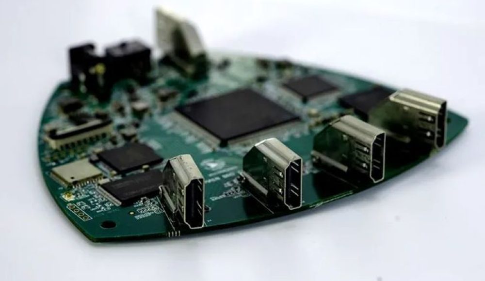
Communication equipment is becoming faster, more compact, and more demanding to manufacture. From 5G radio units and wireless gateways to Ethernet switches, optical network equipment, and industrial communication modules, printed circuit board assemblies must maintain stable electrical performance under increasingly complex operating conditions.
According to the Ericsson Mobility Report published in June 2026, global 5G subscriptions reached approximately 3.1 billion in the first quarter of 2026. Ericsson also forecasts 6.4 billion 5G subscriptions by 2031. These figures illustrate the continued expansion of mobile connectivity, although they do not directly represent demand for communication PCB assemblies.
For OEMs, the challenge is clear: selecting a PCBA Manufacturer that understands high-speed design constraints, RF performance, manufacturing accuracy, and application-specific testing.
Why Communication PCBA Manufacturing Is Different
Communication PCBA manufacturing often involves tighter electrical requirements than conventional low-speed electronics.
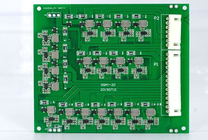
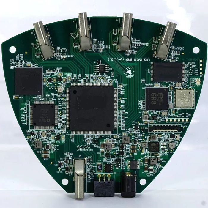
A typical communication board may combine processors, memory, Ethernet PHYs, RF transceivers, power management circuits, high-speed connectors, and sensitive analog components.
These devices must operate together while minimizing signal distortion, electromagnetic interference, and excessive power consumption.
Furthermore, communication equipment may operate continuously in data centers, network cabinets, outdoor installations, or industrial environments.
Therefore, PCB fabrication, component placement, soldering quality, and thermal management must be considered as parts of the same manufacturing system.
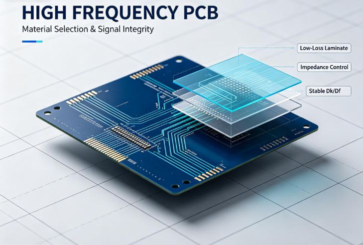
Controlled Impedance and PCB Stackup Design
Signal integrity begins with the PCB stackup.
High-speed communication interfaces rely on controlled transmission-line characteristics. Inappropriate dielectric thickness, copper geometry, or reference-plane configuration can create impedance discontinuities and signal reflections.
For example, Ethernet, high-speed serial links, and RF transmission lines may require defined impedance targets.
A qualified PCB Manufacturer should evaluate dielectric materials, layer arrangements, trace geometry, copper thickness, and manufacturing tolerances.
The manufacturer should also clarify how impedance is calculated, verified, and documented.
In some applications, impedance coupons and test reports may be required.
Importantly, controlled impedance is not simply a design-file requirement. It depends on the ability of the PCB factory to reproduce the specified structure consistently.
Material Selection for High-Frequency Applications
Standard FR-4 materials are suitable for many communication products. However, higher-frequency or lower-loss applications may require specialized laminates.
Material selection should consider dielectric constant (Dk), dissipation factor (Df), operating frequency, temperature, moisture sensitivity, and manufacturing compatibility.
For RF circuits, variations in dielectric properties can affect transmission-line behavior.
Meanwhile, high-speed digital circuits may be sensitive to insertion loss, impedance variation, and via-related discontinuities.
Therefore, OEMs should share material requirements and electrical performance targets before fabrication begins.
An experienced manufacturer can review whether the specified materials and stackup are compatible with the intended production process.
BGA and Fine-Pitch Assembly Challenges
Modern communication PCBAs frequently use dense packages such as BGAs, QFNs, and fine-pitch ICs.
These components enable compact layouts and high interconnection density, but they also increase assembly complexity.
Solder paste printing, placement accuracy, reflow profiling, moisture-sensitive component handling, and PCB warpage control become important manufacturing considerations.
For example, BGA solder joints are hidden beneath the package and cannot be fully evaluated through conventional visual inspection.
Consequently, X-ray inspection may be required to examine solder joint conditions, while AOI can identify visible placement and soldering defects elsewhere on the assembly.
The inspection plan should reflect component complexity rather than applying the same procedure to every product.
Thermal Management and Power Integrity
Communication equipment often contains high-performance processors, RF power amplifiers, and power conversion circuits.
These components can generate significant heat during continuous operation.
Poor thermal management may affect electrical stability, component lifetime, and overall equipment reliability.
Engineers should consider copper distribution, thermal vias, heat-spreading structures, component placement, and enclosure-level cooling.
Meanwhile, manufacturing teams must control soldering quality beneath thermal pads and other heat-transfer interfaces.
Power integrity is equally important.
Insufficient decoupling, poor return-current paths, or excessive power-distribution impedance can introduce noise into sensitive communication circuits.
As a result, electrical design and manufacturing process reviews should be coordinated before production.
Inspection and Testing for Communication PCBAs
Communication PCBA testing should extend beyond checking whether the board powers on.
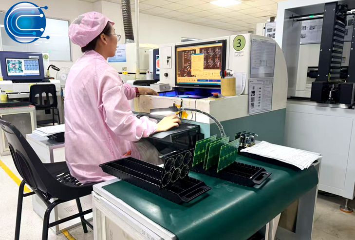
A layered inspection strategy may include solder paste inspection, AOI, X-ray, electrical testing, and functional verification.
Depending on the product, functional testing may evaluate Ethernet link negotiation, data throughput, packet errors, interface communication, RF performance, or power consumption.
RF products may also require specialized measurements such as output power, frequency accuracy, sensitivity, or error vector magnitude.
These tests require suitable equipment, fixtures, and customer-defined acceptance limits.
A PCBA Manufacturer should therefore confirm test requirements during quotation and engineering review.
Not every EMS provider maintains every specialized RF test system internally, so the division of testing responsibilities must be clearly established.
Manufacturing Standards and Process Consistency
Communication PCBAs benefit from documented workmanship criteria and controlled assembly processes.
IPC J-STD-001J addresses soldering materials and processes, while IPC-A-610J provides electronic assembly acceptance criteria.
However, standards alone do not guarantee electrical performance.
Manufacturers must also maintain process controls, revision management, inspection records, and corrective-action procedures.
For high-speed products, even small changes in PCB material, stackup, component selection, or assembly process may require additional validation.
Therefore, engineering changes should be evaluated before being introduced into production.
From Prototype Validation to Volume Production
A communication board that performs correctly during prototype testing may still encounter problems during volume manufacturing.
Differences in materials, fabrication tolerances, component availability, or assembly conditions can affect repeatability.
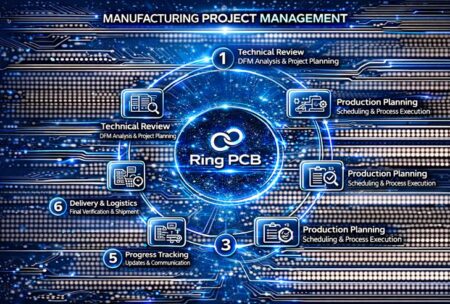
For this reason, pilot production should validate manufacturing processes, test fixtures, inspection coverage, and documentation before larger quantities are released.
A full-turnkey assembly service can improve coordination between PCB fabrication, sourcing, assembly, and testing.
This integrated workflow helps engineering teams identify potential manufacturing issues before they affect delivery schedules.
Supporting Communication PCBA Projects With Ring PCB
Successful communication PCBA manufacturing requires coordinated control of PCB materials, signal integrity, component sourcing, assembly quality, and testing.
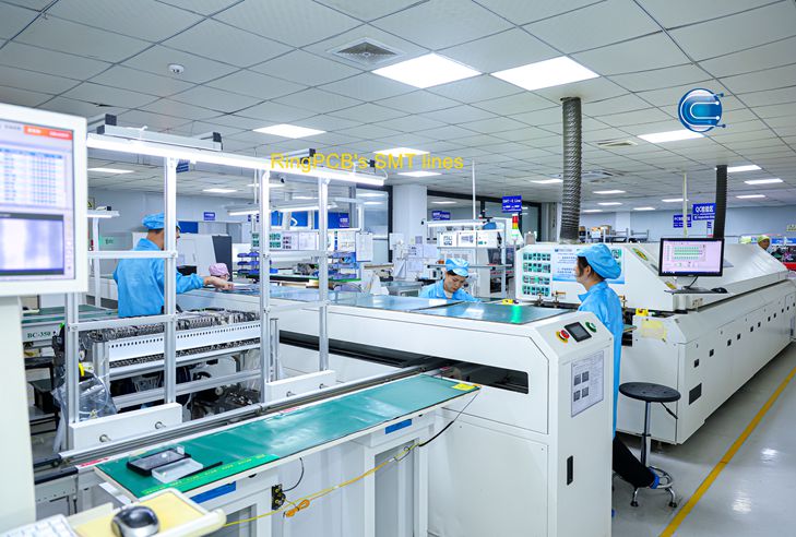
Ring PCB supports communication electronics through multilayer and high-frequency PCB fabrication, component procurement, SMT and THT assembly, engineering review, AOI and X-ray inspection, and full-turnkey assembly services.
For projects involving Ethernet modules, wireless communication equipment, network controllers, or other communication electronics, early manufacturing review can help identify potential risks before production begins.
To discuss your communication PCBA project, send your Gerber files, BOM, stackup requirements, assembly drawings, and testing specifications to rfq@ringpcb.com.
References
- Ericsson. Ericsson Mobility Report: 5G Subscriptions Top Three Billion as Uplink Gains Momentum. June 16, 2026.
- IPC. IPC Releases “J” Revisions to Two Leading Standards for Electronics Assembly. April 8, 2024.
- Ring PCB. PCB Manufacturing and Assembly Services.
https://www.ringpcb.com/