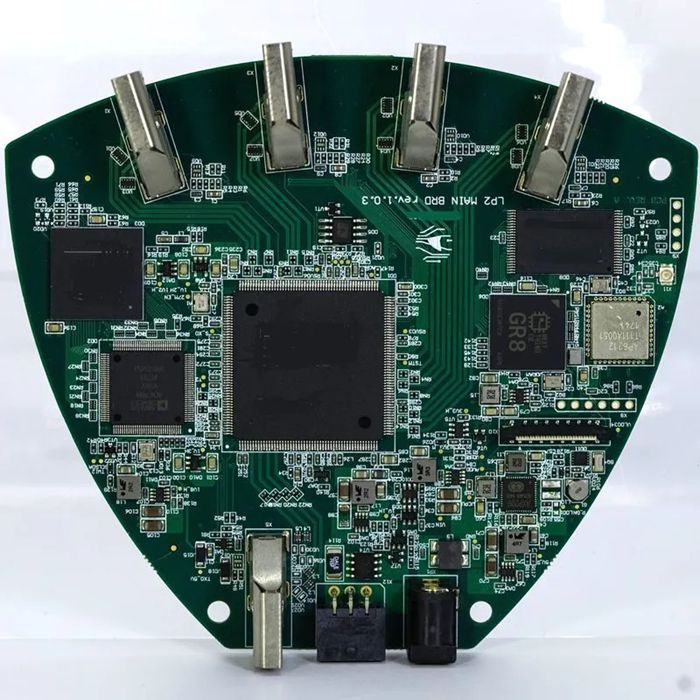
A communication PCB can perform perfectly in an engineering laboratory yet experience intermittent failures after entering volume production. The reason is often not a single defective component, but an interaction between high-speed circuit requirements, PCB fabrication tolerances, assembly variation, and incomplete testing.
For manufacturers of Ethernet switches, wireless gateways, optical networking equipment, and communication modules, this creates a critical challenge: how can high-speed performance remain consistent across hundreds or thousands of assemblies?
According to Ericsson’s June 2026 Mobility Report, global 5G subscriptions reached approximately 3.1 billion in the first quarter of 2026. Meanwhile, mobile network traffic increased 22% year over year during the same period.
Although these figures do not directly measure PCBA demand, they illustrate the increasing performance requirements placed on communication infrastructure.
For OEMs, reliable High-Speed PCB Assembly begins with translating electrical design requirements into repeatable manufacturing controls.
The Hidden Gap Between PCB Design and Manufacturing
High-speed PCB design typically focuses on impedance, insertion loss, crosstalk, timing, and power integrity.
However, the finished board must reproduce the intended electrical structures within real manufacturing tolerances.
For example, a transmission line designed for a particular impedance depends on trace geometry, dielectric thickness, copper characteristics, and reference-plane configuration.
If these parameters change during fabrication, the actual electrical behavior may differ from the simulation.
Therefore, communication PCBA projects should include a manufacturing review before PCB production begins.
This review connects electrical specifications with available materials, fabrication processes, and inspection methods.
Controlled Impedance Requires More Than a Target Value
A drawing that specifies 50-ohm single-ended impedance or 100-ohm differential impedance provides an important requirement, but it does not fully define the manufacturing process.
The PCB Manufacturer must also understand the approved stackup, laminate properties, copper thickness, trace dimensions, and permitted tolerances.
Impedance coupons may be used to verify selected transmission-line structures.
However, coupon testing should be supported by appropriate stackup control and documented fabrication parameters.
For OEMs, the key question is not simply whether a factory offers controlled impedance.
It is whether the factory can consistently manufacture the approved structure and communicate deviations before production.
Material Selection and Insertion Loss
Communication PCB materials must be selected according to operating frequency, channel length, thermal requirements, and electrical performance.
Standard FR-4 may be suitable for many digital communication applications.
For more demanding high-frequency or low-loss applications, specialized laminates may be necessary.
Important parameters include dielectric constant, dissipation factor, glass transition temperature, and dimensional stability.
Material availability also matters.
An unapproved laminate substitution can affect impedance, insertion loss, and qualification results.
Consequently, critical material specifications should remain controlled throughout prototype and volume production.
Via Structures and High-Speed Transitions
Vias allow signals to move between PCB layers, but they can also introduce electrical discontinuities.
At sufficiently high frequencies, unused via stubs may contribute to reflections and signal degradation.
Backdrilling, blind vias, or other structures may help address specific channel requirements.
However, these techniques introduce additional manufacturing considerations involving drilling accuracy, plating reliability, and inspection.
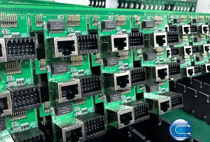
Similarly, connector transitions and BGA escape routing can influence channel performance.
The appropriate solution depends on the actual signal requirements rather than applying advanced PCB structures unnecessarily.
A qualified PCBA Manufacturer should coordinate fabrication feasibility with the OEM’s electrical specifications.
BGA Assembly and Manufacturing Repeatability
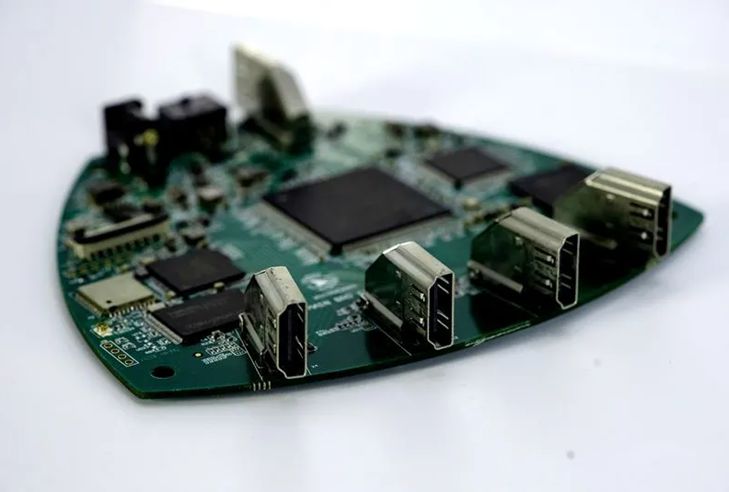
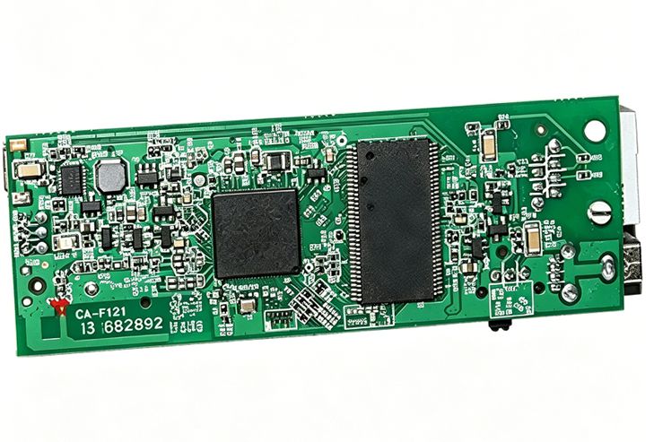
Communication PCBAs often contain processors, memory devices, Ethernet controllers, and high-density packages.
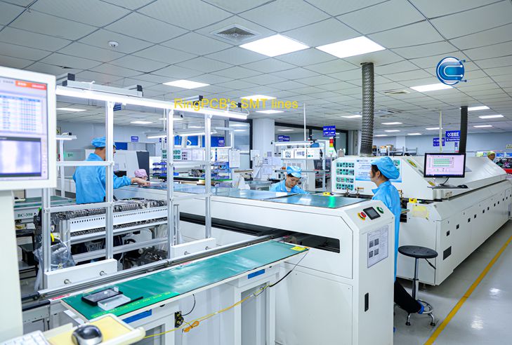
BGAs and fine-pitch components require precise solder paste printing, placement, and reflow control.
PCB warpage, package moisture sensitivity, and uneven heating may contribute to soldering defects.
Solder paste inspection can identify deposition problems before placement.
AOI detects visible assembly defects, while X-ray inspection can help evaluate hidden BGA solder joints.
Nevertheless, inspection results must be interpreted according to the component and process requirements.
A visually acceptable assembly is not automatically a functionally verified communication product.
Test the Signals That Matter
A board that powers on successfully may still contain high-speed performance problems.
For this reason, functional test plans should reflect the intended application.
Depending on the product, testing may include Ethernet communication, interface throughput, packet error monitoring, firmware programming, or power consumption verification.
More demanding applications may require bit error rate measurements, eye-diagram analysis, or other specialized signal-integrity tests.
RF products may require frequency, output power, sensitivity, or modulation measurements.
Not every PCBA factory performs these specialized tests internally.
OEMs should therefore agree on test equipment, fixtures, acceptance criteria, and responsibilities before production.
Pilot Production Reveals Process Variation
Engineering prototypes are useful for validating design functionality, but they do not always represent volume manufacturing conditions.
A pilot build can reveal variation in PCB fabrication, soldering, component sourcing, and testing.
For example, an assembly may pass initial tests but exhibit intermittent communication failures after thermal cycling.
Such results should trigger a structured investigation rather than immediate assumptions about the root cause.
Potential contributors include solder joints, connector interfaces, thermal expansion, power integrity, or electrical design margins.
Pilot production allows these risks to be evaluated before larger manufacturing commitments.
Engineering Change Control Protects Signal Integrity
Communication equipment frequently undergoes component updates and PCB revisions.
However, changing a laminate, connector, oscillator, or critical passive component can affect performance.
Therefore, approved changes should be evaluated for electrical, mechanical, and manufacturing consequences.
Revision control should synchronize Gerber files, stackup documents, BOM data, assembly instructions, and test procedures.
A full-turnkey assembly service can simplify coordination across these activities.
This is particularly valuable when fabrication and assembly teams need to implement the same engineering revision.
Manufacturing High-Speed Communication PCBAs With Ring PCB
Reliable high-speed communication electronics depend on consistent PCB fabrication, controlled assembly processes, and appropriate verification.
Ring PCB supports communication projects through multilayer and high-frequency PCB fabrication, controlled-impedance manufacturing, component sourcing, SMT and THT assembly, engineering review, inspection, and full-turnkey PCBA services.
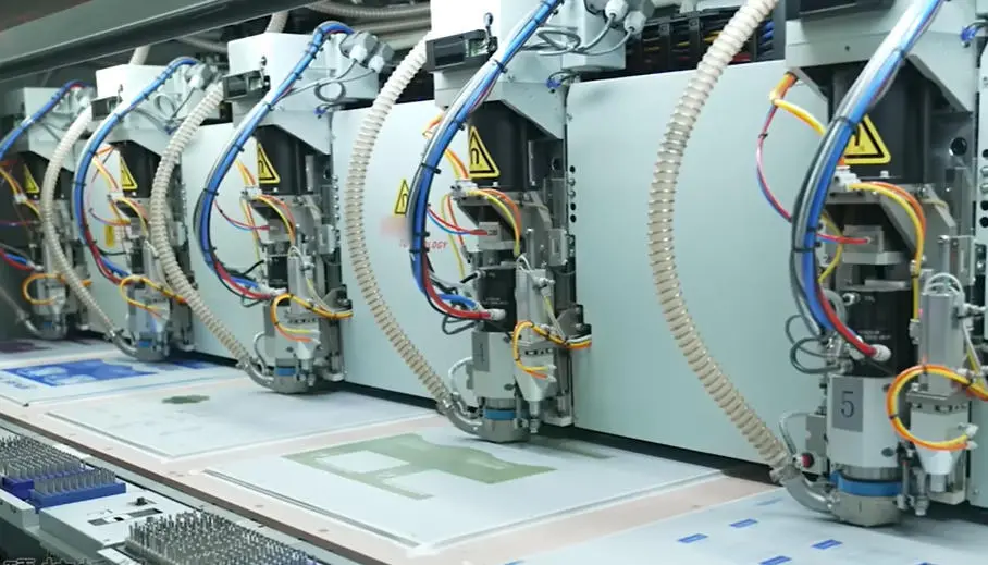
For OEMs developing networking equipment, communication modules, and other high-speed electronic assemblies, early manufacturing collaboration can help identify risks involving materials, stackup, component availability, and assembly processes.
To request a manufacturing review or quotation, send your Gerber or ODB++ files, BOM, stackup requirements, quantities, and testing specifications to rfq@ringpcb.com.
References
- Ericsson. Ericsson Mobility Report: 5G Subscriptions Top Three Billion as Uplink Gains Momentum. June 16, 2026.
- Ring PCB. Custom Controlled Impedance High Speed PCB. Technical manufacturing information.
- Ring PCB. FR-4 Communication PCBA. Communication electronics manufacturing information.
https://www.ringpcb.com/product/fr-4-communication-pcba/