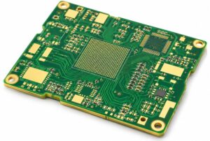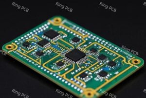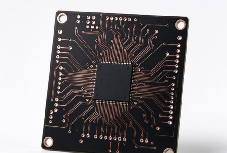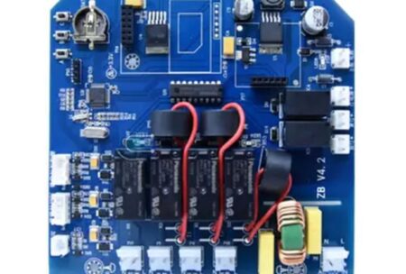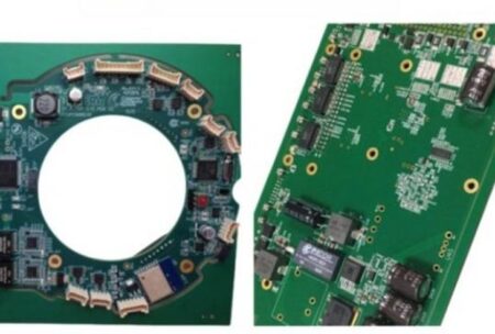

As electronic products become more integrated, a single or double-sided PCB may no longer provide enough routing space for all required circuits. Multilayer PCBs solve this problem by combining multiple conductive layers separated by insulating dielectric materials. They allow engineers to distribute signal, ground, and power networks across a compact board structure.
However, adding more layers also increases manufacturing complexity. Layer alignment, copper distribution, dielectric thickness, drilling, lamination, and electrical performance must all be controlled as one manufacturing system.
For OEM purchasing teams and hardware engineers, understanding these factors is essential when selecting a multilayer PCB manufacturer. A board that looks correct in the layout file may still present production risks if its stackup is not compatible with the fabricator’s process capability.
This article examines the key stages and decisions involved in multilayer PCB manufacturing, from stackup planning to production inspection.
1. Why Use a Multilayer PCB?
A multilayer PCB contains three or more conductive copper layers laminated together with insulating materials. Depending on the application, these layers may be assigned to signal routing, ground reference, power distribution, or a combination of functions.
Compared with a two-layer board, a multilayer construction can offer several advantages:
- More routing capacity within the same board footprint
- Dedicated ground and power planes
- Improved options for electromagnetic compatibility
- Shorter or more organized signal-routing paths
- Better support for complex component layouts
- Greater integration in compact electronic products
Multilayer boards are widely used in industrial control systems, communication equipment, medical electronics, computing hardware, and automotive electronics.
Nevertheless, higher layer counts should be selected according to actual electrical and mechanical requirements. More layers can increase material consumption, drilling operations, lamination cycles, and inspection demands.
2. Stackup Design: The Foundation of Manufacturing
The stackup defines the sequence of copper layers and dielectric materials in the finished PCB. It influences board thickness, impedance, signal return paths, mechanical balance, and manufacturing cost.
A typical multilayer stackup includes copper foil, prepreg, and one or more core materials. During lamination, heat and pressure bond these materials into a single board structure.
A good stackup should address several factors:
Layer allocation: Signal layers should be assigned with reference planes and routing requirements in mind. High-speed signals often benefit from a continuous reference plane close to the signal layer.
Dielectric thickness: The spacing between copper layers affects impedance and capacitance. It also influences the finished board thickness and via geometry.
Copper thickness: Copper weight affects current-carrying capability, etching behavior, and the dimensions of finished traces.
Symmetry and balance: A balanced construction can help reduce uneven stress and dimensional distortion during lamination and cooling.
Therefore, stackup selection should not be based only on reaching a target layer count. It should reflect the electrical requirements and the manufacturing process that will produce the board.
3. Material Selection: Core, Prepreg and Copper Foil
Material selection is another major decision in multilayer PCB manufacturing. The laminate and prepreg system determines dielectric properties, thermal behavior, mechanical stability, and compatibility with the fabrication process.
FR-4 is widely used because it offers a practical balance of cost, electrical performance, and manufacturability. However, not every FR-4 material has identical properties. Different grades can vary in glass transition temperature, dielectric constant, dissipation factor, thermal expansion, and moisture performance.
For more demanding applications, engineers may consider specialized materials from suppliers such as Panasonic, Rogers, Taconic, or ISOLA, depending on the required electrical and thermal characteristics.
The selection should be driven by measurable project requirements rather than brand preference alone. Buyers should confirm the exact material grade, thickness, copper weight, and applicable material specification with the PCB manufacturer.
In addition, the compatibility of different materials within a hybrid stackup should be reviewed carefully. Differences in thermal expansion and lamination behavior can affect registration and long-term reliability.
4. Inner-Layer Imaging and Etching
Before the multilayer board is laminated, the inner-layer copper patterns must be transferred and etched.
The process typically includes surface preparation, photoresist coating, imaging, developing, etching, and stripping. The objective is to produce the intended copper traces and spaces while maintaining dimensional accuracy.
As conductor widths and spacing become smaller, process control becomes increasingly important. Over-etching can reduce trace width, while under-etching can leave unwanted copper between conductors.
The manufacturer must also consider copper thickness. Heavier copper generally requires different etching compensation and process control from thinner copper.
For multilayer projects, inner-layer inspection is important because defects may become inaccessible after lamination. Any short circuits, open circuits, or pattern defects that remain undetected can affect the finished board.
5. Layup and Lamination: Building the Multilayer Structure
After inner-layer circuits are prepared and inspected, the layers are arranged in the specified sequence with prepreg and copper foil. This is commonly referred to as layup.
The assembled materials then enter the lamination process, where controlled heat and pressure cause the resin to flow and bond the layers together.
Several variables influence the result:
- Lamination temperature and pressure profile
- Resin flow and curing behavior
- Prepreg thickness and resin content
- Copper distribution across layers
- Material alignment and dimensional stability
If the process is not properly matched to the material system, defects such as delamination, voids, resin starvation, or dimensional distortion may occur.
Layer registration is particularly important in high-layer-count boards. Misalignment can reduce annular rings around drilled holes or affect the intended connection between layers.
For this reason, the stackup, tooling, material data, and lamination sequence should be reviewed before production rather than treated as independent details.
6. Drilling, Plating and Interlayer Connections
Once lamination is complete, holes are drilled to create electrical connections between designated copper layers.
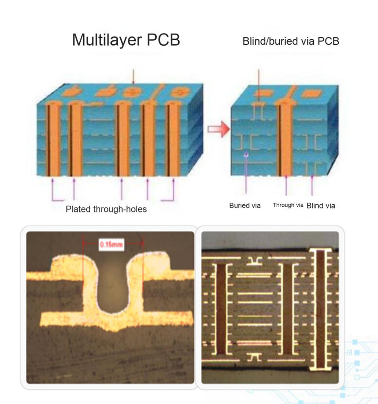
Mechanical drilling is commonly used for plated through-holes. Depending on the board construction, blind vias and buried vias may also be required.
A blind via connects an outer layer to an inner layer, while a buried via connects internal layers without reaching the external surfaces. These structures can release routing space, but they also introduce additional manufacturing steps and design constraints.
After drilling, hole-wall preparation and metallization are required to establish conductive connections. Copper plating forms the conductive barrel inside plated through-holes and builds up copper on the board surfaces.
For high-layer-count boards, drill aspect ratio, hole diameter, copper plating quality, and registration should be considered together. A very thick board with small drilled holes can create a more demanding plating process.
Where the design requires it, backdrilling may remove unused portions of plated via barrels. This can reduce via-stub effects in high-speed signal paths, although it is a separate process decision rather than a standard requirement for every multilayer PCB.
7. Common Multilayer PCB Manufacturing Risks
Several problems can affect multilayer board quality and production yield.
Layer misregistration: Incorrect alignment between layers can reduce annular ring dimensions or create unwanted connections.
Delamination: Inadequate bonding or incompatible material behavior can weaken the laminate structure.
Insufficient plating: Poor copper coverage inside drilled holes can affect electrical continuity and reliability.
Impedance variation: Changes in dielectric thickness, trace width, or copper geometry can shift the finished impedance.
Board warpage: Uneven copper distribution, material imbalance, or lamination stress can cause dimensional distortion.
Internal shorts or opens: Inner-layer pattern defects may become difficult to repair after the board is laminated.
To manage these risks, OEMs should provide complete fabrication documentation and agree on the applicable acceptance criteria before production.
8. What Buyers Should Include in an RFQ
A complete quotation package helps the manufacturer evaluate the project accurately. It should include:
- Gerber or other agreed fabrication data
- Layer count and stackup drawing
- Finished board thickness and tolerance
- Copper weight for each layer
- Material grade and dielectric requirements
- Hole sizes, via types, and aspect-ratio requirements
- Surface finish and solder mask specifications
- Impedance requirements, if applicable
- Board dimensions, quantity, and delivery expectations
- Applicable industry standards and customer-specific requirements
If the PCB will also be assembled, the BOM, assembly drawings, and component requirements should be provided for a separate PCBA review.
Multilayer PCB Manufacturing with Ring PCB
Ring PCB provides multilayer PCB fabrication with a published capability of up to 30 layers for mass production and up to 70 layers for samples. Its process capability also lists finished board thickness ranges of 0.3–6.0 mm for mass production and 0.2–10 mm for samples.
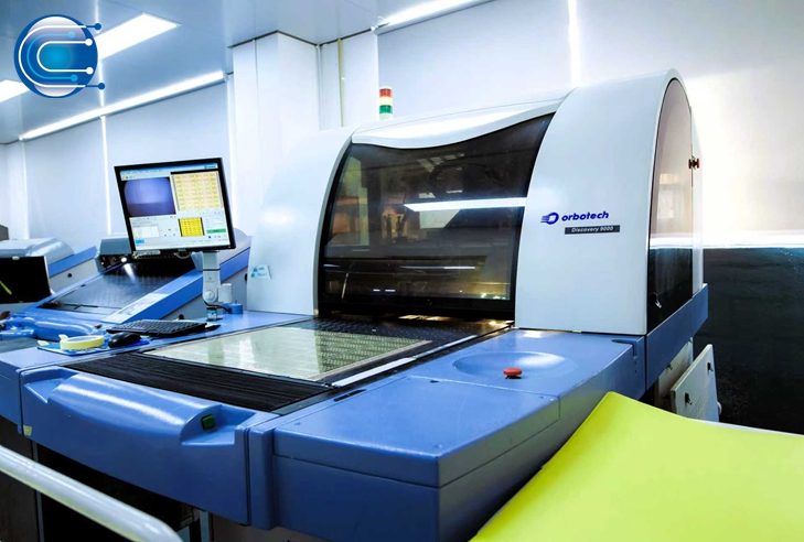
The manufacturing portfolio includes high-layer-count, hybrid, heavy-copper, HDI, rigid-flex, stepped, and other specialized PCB types, subject to project review. Available material options include FR-4-related suppliers and specialized laminate brands such as Panasonic, Rogers, Taconic, and ISOLA.
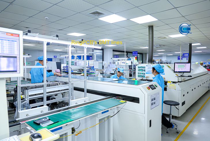
Beyond bare-board fabrication, Ring PCB supports component sourcing, SMT and through-hole assembly, and production quality inspection. This allows customers to coordinate PCB fabrication and assembly requirements within one manufacturing workflow.
For an accurate quotation, customers can submit Gerber files, stackup details, board specifications, quantities, and any customer-specific requirements. Ring PCB reviews the manufacturing information and discusses feasibility before confirming the project.
Contact rfq@ringpcb.com to discuss your multilayer PCB requirements.
References and Further Reading
- IPC — IPC-6012, Qualification and Performance Specification for Rigid Printed Boards.
- IPC — IPC-4101, Specification for Base Materials for Rigid and Multilayer Printed Boards.
- IPC — IPC-2221, Generic Standard on Printed Board Design.
- Ring PCB — Multilayer PCB Stackup Design: From DFM Review to Reliable Manufacturing.
- Altium Resources — High-Density Interconnects: A Design and Manufacturing Guidebook.