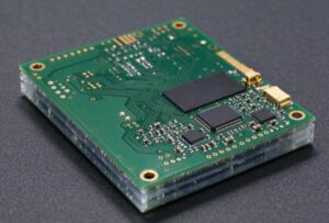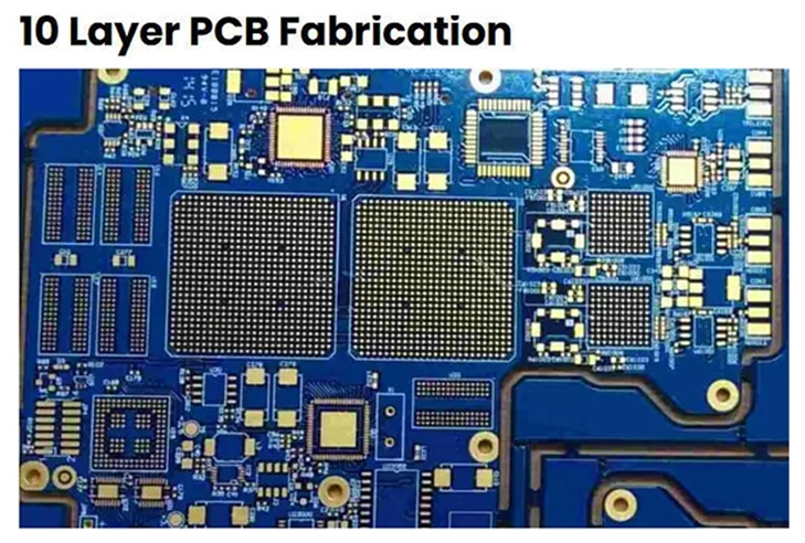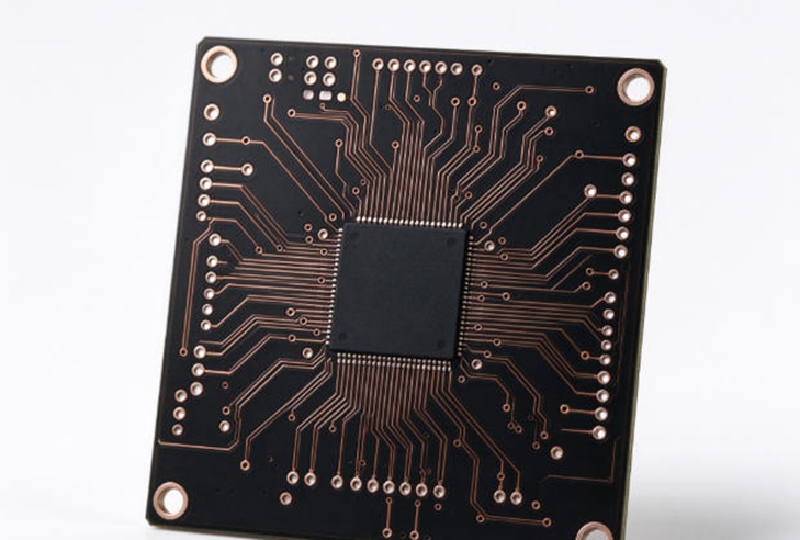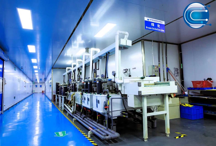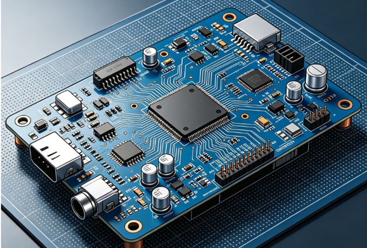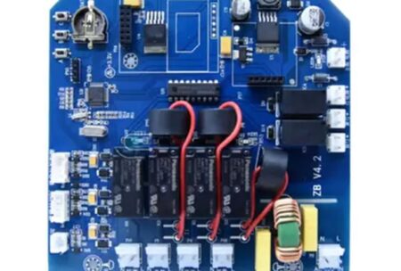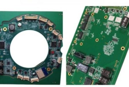

Multilayer PCB manufacturing involves a sequence of interconnected processes, from inner-layer imaging and etching to lamination, drilling, plating, solder mask application, and final inspection. Each stage must meet the specified design requirements because a defect introduced early in production may affect several downstream processes.
For OEM purchasing teams, manufacturing yield and lead time are closely connected. A design that is difficult to fabricate can require additional engineering clarification, process adjustments, or rework. Similarly, incomplete documentation and late engineering changes can delay production even when factory capacity is available.
As multilayer boards become more complex, manufacturers must coordinate material selection, layer registration, drilling accuracy, copper plating, and quality verification with greater precision.
This article examines seven factors that influence multilayer PCB manufacturing performance and explains what buyers should review before placing an order.
1. Design Data Quality and DFM Readiness
The manufacturing process begins with the customer’s design data.
Gerber files, drill files, stackup information, fabrication drawings, and technical specifications must describe the same PCB revision. Missing or inconsistent information can create questions about board thickness, copper weight, hole dimensions, surface finish, or impedance requirements.
A Design for Manufacturability (DFM)) review helps identify potential conflicts before production.

Common review items include:
- Minimum trace width and spacing
- Annular ring and pad dimensions
- Drill sizes and via structures
- Copper-to-edge clearance
- Board thickness and tolerance
- Solder mask openings
- Surface finish requirements
- Controlled-impedance specifications
The customer should also identify which parameters are critical to product performance and which may be adjusted following engineering approval.
A clear and complete fabrication package reduces unnecessary communication and helps the supplier prepare a more accurate quotation.
2. Inner-Layer Imaging and Etching Accuracy
Multilayer PCB manufacturing begins with the preparation of individual copper-clad layers.
The inner-layer imaging process transfers the required circuit pattern onto the copper surface. Unwanted copper is then removed through etching to create the specified conductive traces and planes.
The quality of this stage influences the final conductor geometry and electrical connectivity.
Potential issues include under-etching, over-etching, insufficient spacing, and defects in the copper pattern. These problems may lead to shorts, opens, or dimensional deviations.
The challenge increases when the design combines fine lines with heavier copper. Thicker copper may require greater etching compensation and tighter process control to maintain the intended trace dimensions.
For buyers, the key question is whether the manufacturer’s process capability matches the actual copper weight and minimum line-and-space requirements in the Gerber data.
3. Layer Registration and Lamination Control
Lamination is one of the most important stages in multilayer PCB manufacturing.
Prepared inner layers are stacked with insulating materials and copper foil according to the approved stackup. Heat and pressure are applied under controlled conditions to bond the layers into a solid structure.
Accurate layer alignment is essential. Misregistration can reduce annular ring margins, affect via connections, or create clearance problems between conductive features.
Other potential risks include resin voids, delamination, thickness variation, and warpage.
Manufacturers must manage several variables, including:
Material Compatibility: Prepreg and core materials should be suitable for the required electrical, thermal, and mechanical conditions.
Stackup Symmetry: Balanced construction can help reduce dimensional distortion and warpage.
Pressing Parameters: Temperature, pressure, and curing conditions must match the material system and board construction.
Registration Accuracy: Layer alignment must remain within the specified tolerances.
For complex multilayer boards, customers should provide a complete stackup drawing and confirm the required finished thickness and tolerances before production.
4. Drilling and Plated Through-Hole Quality
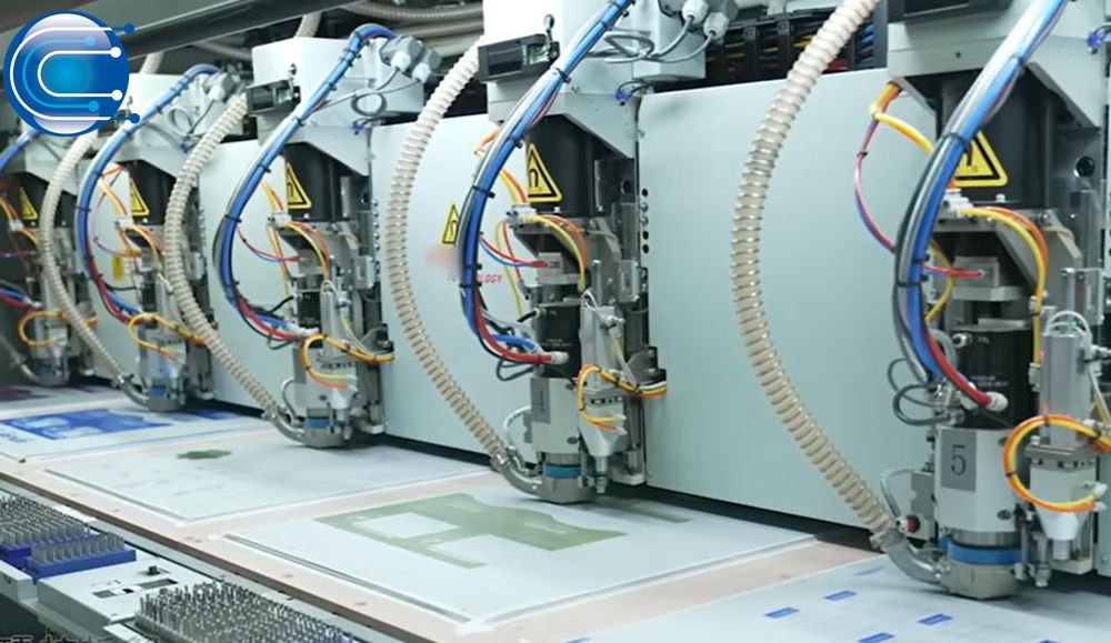
After lamination, holes are drilled to establish interconnections between layers and provide mounting locations for components.
Mechanical drilling is commonly used for through-holes and many conventional vias. Laser drilling may be used for selected HDI microvia structures.
Drilling quality affects hole-wall condition, registration, and subsequent copper plating.
The plated through-hole process deposits copper onto the hole walls to establish electrical connections between the relevant layers. Inadequate plating or poor hole-wall preparation may compromise electrical continuity and reliability.
Important manufacturing considerations include:
- Drill registration
- Finished hole diameter
- Aspect ratio
- Hole-wall preparation
- Copper plating thickness
- Annular ring integrity
- Via structure and layer span
For demanding applications, buyers should clarify the applicable plated-hole requirements and any additional reliability testing specified in the purchase documentation.
5. Copper Plating and Electrical Interconnection
Copper plating forms the conductive connection within drilled holes and contributes to the final copper structure.
The process must achieve the required coverage and thickness while maintaining consistency across the panel.
High-aspect-ratio holes can be more challenging because the hole geometry affects solution exchange and copper deposition. Complex via structures may also require additional process controls.
For multilayer PCBs, the quality of these interconnections is critical. A board can appear visually acceptable while still requiring electrical verification to confirm continuity.
Depending on the product requirements, manufacturing verification may include electrical testing, microsection analysis, and other specified process checks.
The customer should define the required acceptance criteria and testing scope rather than relying on a generic statement that the PCB has been inspected.
6. Material, Surface Finish, and Dimensional Stability
Material selection and surface finish can affect both manufacturing yield and the suitability of the PCB for its end application.
FR-4 materials are widely used for general multilayer boards, but different grades have different thermal and electrical properties. High-speed, high-temperature, or specialized applications may require a particular material system.
Surface finish selection also matters.
ENIG offers a relatively flat surface and is commonly selected for fine-pitch assembly. Lead-free HASL, immersion silver, OSP, and other finishes may be suitable depending on soldering, storage, contact, and application requirements.
Dimensional stability should also be considered. Board thickness, copper distribution, material expansion, and panel design can affect finished dimensions and warpage.
The supplier should confirm that the selected material and finish are compatible with the design and assembly process.
7. Inspection Planning and Production Yield Management
Inspection should be integrated into the manufacturing process rather than treated only as a final step.
Depending on the PCB specification, verification may include:
- Inner-layer imaging inspection
- Automated optical inspection
- Layer registration checks
- Plated-hole inspection
- Microsection analysis
- Electrical continuity and isolation testing
- Finished thickness and dimensional measurement
- Surface finish inspection
Each method checks different characteristics. For example, AOI can identify certain visible pattern defects, while microsection analysis can reveal internal construction details. Electrical testing checks defined connectivity and isolation conditions.
IPC-6012 specifies qualification and performance requirements for rigid printed boards. IPC-A-600 provides visual acceptance guidance. The required class, revision, and any customer-specific criteria should be agreed before production.
Manufacturers should also review defect trends and process data to identify recurring issues. This can help improve consistency across repeat orders.
8. What Buyers Can Do to Reduce Lead-Time Risks
Manufacturing lead time depends on more than the factory’s nominal production schedule.
Material availability, board complexity, engineering clarification, process sequence, inspection requirements, and order quantity can all affect delivery.
To improve planning, buyers should:
- Submit complete and consistent fabrication data.
- Confirm material grade and copper requirements early.
- Identify controlled-impedance and special via requirements.
- Review the supplier’s manufacturing limits before order placement.
- Approve engineering questions and proposed changes promptly.
- Confirm inspection and acceptance requirements before production.
- Separate prototype planning from repeat mass-production planning.
A realistic schedule should be based on the actual board construction and material availability rather than a general lead-time promise.
Multilayer PCB Manufacturing at Ring PCB
Ring PCB has provided PCB and PCBA manufacturing services since 2008. Its self-owned 10,000+ square meter facility and approximately 500 employees support PCB production and assembly projects for global customers.
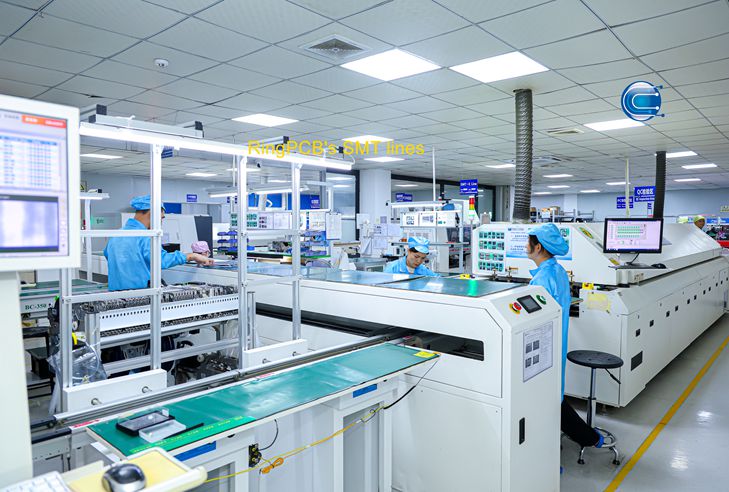
The company offers PCB manufacturing up to 62 layers, with monthly bare PCB production capacity of up to 50,000 square meters. Its manufacturing resources include advanced imaging, CNC drilling, lamination, and inspection equipment to support different PCB constructions.
In addition to bare PCB fabrication, Ring PCB provides component sourcing, SMT assembly, through-hole assembly, and production quality inspection. Customers can submit Gerber files, drill data, stackup drawings, and specific technical requirements for manufacturing review before order confirmation.
For multilayer PCB quotations and manufacturing discussions, contact rfq@ringpcb.com.
References and Further Reading
- IPC — IPC-6012: Qualification and Performance Specification for Rigid Printed Boards.
- IPC — IPC-A-600: Acceptability of Printed Boards.
- IPC — IPC-2221: Generic Standard on Printed Board Design.
- IPC — IPC-TM-650: Test Methods Manual.
- IPC — Printed Board Fabrication and Quality Standards.
- ICAPE Group — Global PCB Report, Industry Insights, Q1 2026.