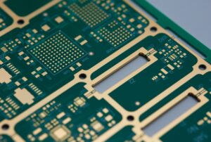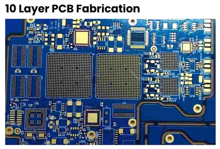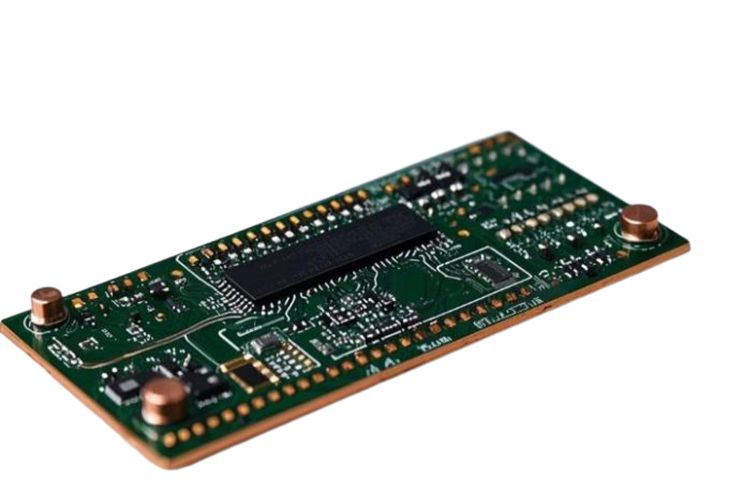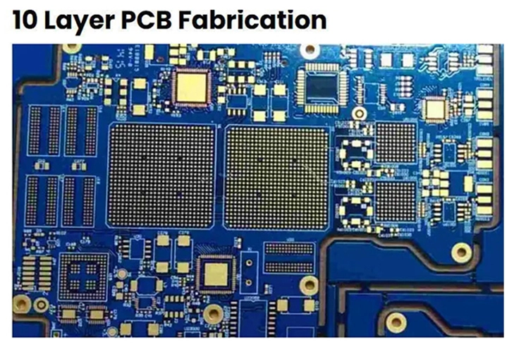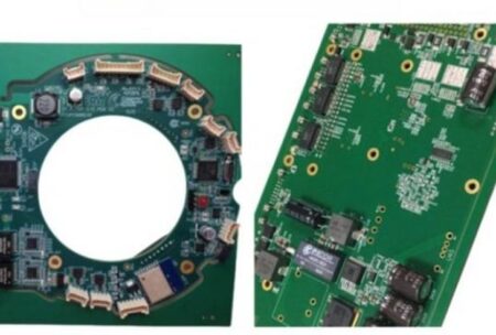
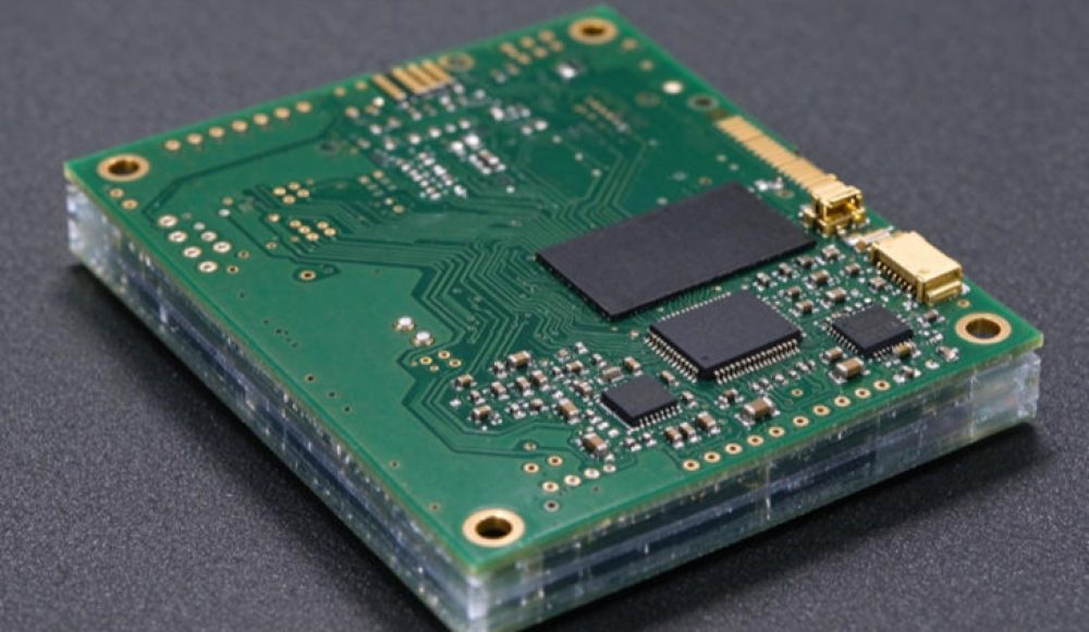
As electronic products become smaller and more functionally integrated, PCB designs must accommodate increasing numbers of components, signal connections, power networks, and control circuits within limited physical space. From industrial automation and communication equipment to medical electronics and automotive systems, multilayer PCBs provide the routing density and structural flexibility required by many complex electronic products.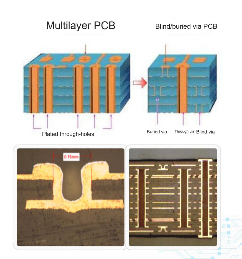
However, choosing a multilayer PCB is not simply a matter of selecting a higher layer count. An unsuitable stackup, material, copper distribution, or manufacturing specification can increase cost, complicate production, and affect long-term reliability.
For OEM engineers and procurement teams, the real challenge is to select a PCB structure that meets electrical and mechanical requirements while remaining practical to manufacture at the required volume.
This guide explains the key considerations when specifying a multilayer PCB and evaluating a manufacturing partner.
1. Start with the Product’s Electrical and Functional Requirements
Before deciding how many layers a PCB needs, define what the board must accomplish.
A multilayer PCB may contain several functional groups, including high-speed signals, low-speed control circuits, power distribution, grounding networks, and sensitive analog interfaces. These functions may require different routing and reference-plane arrangements.
For example, a communication device may prioritize controlled impedance and signal integrity, while an industrial controller may place greater emphasis on power distribution, electrical isolation, and environmental durability. A medical electronic product may have additional requirements for documentation, risk management, and production consistency.
The initial specification should therefore identify:
- Operating voltage and current requirements
- Signal frequency and data-rate requirements
- Controlled-impedance targets, where applicable
- Power and ground distribution needs
- Board dimensions and mechanical constraints
- Operating temperature and environmental conditions
- Expected product lifecycle and production volume
Once these requirements are understood, engineers can determine whether a four-, six-, eight-, or higher-layer construction is appropriate.
2. Select Layer Count Based on Routing Needs, Not Complexity Alone
Adding layers provides additional routing resources, but it also affects material usage, lamination cycles, drilling, registration, and manufacturing cost.
A four-layer PCB may be sufficient for a relatively compact controller with moderate routing requirements. Six- or eight-layer boards can provide more routing flexibility for products with denser component placement, multiple power domains, or more demanding signal-routing requirements.
Higher-layer-count boards are commonly used in communication systems, computing equipment, advanced industrial electronics, and other products with complex interconnections.
Industry data also illustrates the increasing importance of high-layer-count boards. A 2026 industry overview reported that the global revenue of multilayer PCBs with 18 or more layers was approximately US$2.5 billion in 2024 and projected it to reach US$5 billion by 2029. The report identifies this segment as an important growth area associated with AI servers and high-speed networking.
Nevertheless, these market trends should not encourage unnecessary layer additions. A higher layer count is justified only when it solves a real electrical, routing, or mechanical requirement.
3. Evaluate Stackup Structure and Layer Arrangement
The stackup defines how copper layers and insulating materials are arranged throughout the PCB.
A well-planned stackup can support signal routing, reference-plane continuity, power distribution, and mechanical balance. Conversely, a poorly balanced structure may introduce manufacturing and performance problems.
Important considerations include:
Signal and Reference Layers
High-speed signals generally benefit from a suitable reference plane and a controlled return-current path. Routing a signal across an inappropriate plane split may increase return-path discontinuity and electromagnetic interference.
Power and Ground Distribution
Dedicated power and ground planes can simplify distribution and provide useful reference structures. Their placement should reflect the circuit’s current requirements and electrical architecture.
Dielectric Thickness
The distance between copper layers affects impedance and coupling. For controlled-impedance designs, dielectric thickness, material properties, copper geometry, and manufacturing tolerances must be considered together.
Copper Balance
Copper distribution across the stackup should be evaluated to support dimensional stability and reduce the risk of warpage during manufacturing.
The final stackup should be reviewed against the fabrication process available from the selected PCB supplier.
4. Choose the Right Laminate Material
Material selection influences electrical behavior, thermal performance, mechanical properties, and manufacturing cost.
FR-4 remains widely used because it offers a practical balance of electrical, mechanical, and cost characteristics for many electronic applications. However, not all FR-4 materials are identical. Different grades have different glass-transition temperatures, decomposition temperatures, dielectric properties, and thermal expansion characteristics.
For more demanding applications, engineers may consider materials with lower dielectric loss, more stable electrical properties, or improved thermal performance.
The choice should reflect the product’s actual operating conditions rather than a general preference for premium materials.
Before production, the customer should specify the required laminate grade or approved material system, especially when dielectric properties, thermal reliability, or regulatory documentation are important.
5. Consider Via Structures and Interconnection Requirements
Via technology affects routing density, manufacturing complexity, and the connection between PCB layers.
Through-hole vias extend through the complete board and provide a conventional interlayer connection. Blind vias connect an outer layer to one or more internal layers, while buried vias connect internal layers without reaching the outer surfaces.
These structures can help increase routing flexibility in dense designs, but they may require additional drilling, plating, lamination, and registration controls.
For boards with high component density, fine-pitch packages, or restricted routing space, HDI structures and microvias may be worth evaluating. However, their use should be based on a genuine layout requirement because advanced via structures can increase process complexity and cost.
The fabrication package should clearly define via spans, finished hole sizes, plating requirements, and any special construction details.
6. Match Copper Weight to Current and Thermal Requirements
Copper weight is another important selection factor.
Thicker copper can increase conductor cross-sectional area and support higher-current paths. However, current capacity also depends on trace width, conductor length, temperature rise, board construction, and cooling conditions.
Increasing copper thickness may affect fine-line etching, spacing, plating, and finished board dimensions. It is therefore important to review copper requirements together with the minimum trace and space specifications.
For power-related multilayer boards, engineers should also consider the connection between copper planes, component pads, thermal vias, connectors, and external heat-dissipation structures.
A practical design balances electrical performance with fabrication feasibility.
7. Evaluate Reliability and Manufacturing Standards
A multilayer PCB must maintain electrical and mechanical integrity throughout its intended service life.
Potential reliability concerns include interlayer separation, plated-hole defects, poor copper adhesion, warpage, and thermal-expansion stress. These risks are influenced by material selection, stackup design, drilling, plating, lamination, and process control.
For rigid printed boards, IPC-6012 provides qualification and performance requirements, while IPC-A-600 provides visual acceptance guidance. The applicable revision, product class, and additional customer specifications should be clearly identified in the procurement documentation.
Buyers should also ask suppliers how they control layer registration, plated through-hole quality, electrical continuity, dimensional tolerances, and process verification.
A certification or general quality statement alone does not demonstrate that a particular PCB construction is suitable for a specific application. The manufacturing specification and acceptance criteria must be reviewed together.
8. Assess the Supplier’s Capability Before Finalizing the Design
A technically suitable design must also be manufacturable by the selected supplier.
Before issuing an RFQ, provide the Gerber files, stackup information, material requirements, drill data, copper specifications, and expected order quantity.
Ask the manufacturer to confirm:
- Maximum layer count for the requested production category
- Available laminate materials
- Minimum line width and spacing
- Minimum mechanical and laser-drilled hole sizes
- Copper-weight capability
- Finished board thickness tolerance
- Supported via structures
- Surface finish options
- Prototype and mass-production lead-time expectations
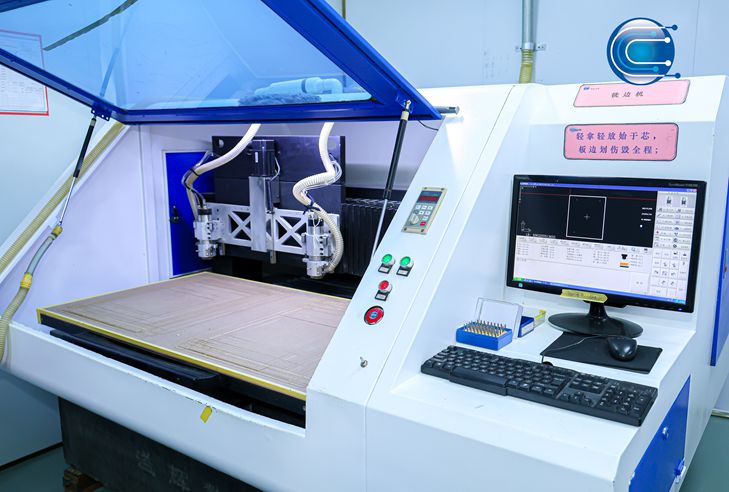
It is also useful to evaluate whether the supplier can support both bare PCB fabrication and subsequent PCBA requirements. Coordinating these stages may simplify production planning and communication.
Multilayer PCB Manufacturing with Ring PCB
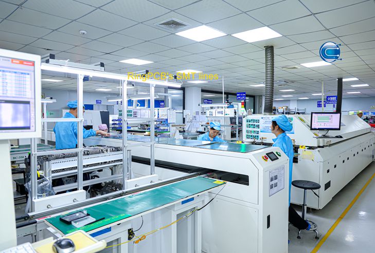
Ring PCB has specialized in PCB fabrication and PCBA manufacturing since 2008. Its self-owned manufacturing facility covers approximately 10,000 square meters and is supported by a team of around 500 employees.

The company provides multilayer PCB fabrication up to 62 layers, together with component sourcing, SMT assembly, through-hole assembly, and production quality inspection. Its monthly bare PCB production capacity reaches 50,000 square meters, supporting projects across different technical requirements and production volumes.
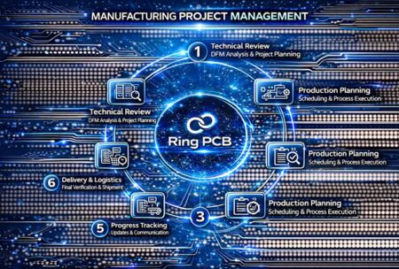
For a new multilayer PCB project, customers can submit Gerber files, stackup information, material specifications, and technical requirements for manufacturing review. Ring PCB can discuss process feasibility and production requirements before order confirmation.
To discuss your multilayer PCB requirements, contact rfq@ringpcb.com.
References and Further Reading
- IPC — IPC-2221: Generic Standard on Printed Board Design.
- IPC — IPC-6012: Qualification and Performance Specification for Rigid Printed Boards.
- IPC — IPC-A-600: Acceptability of Printed Boards.
- Industry overview of multilayer PCB market segmentation and 2024–2029 forecasts, HKEX-listed company industry research, 2026.
- IPC — Printed Board Design and Manufacturing Standards.